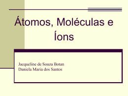
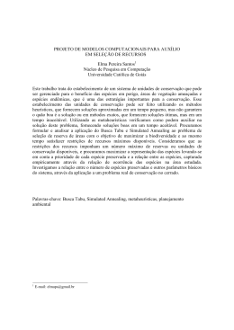
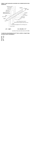
UNIVERSIDADE FEDERAL DO RIO GRANDE DO SUL INSTITUTO DE FÍSICA Análise de materiais nanoestruturados utilizando feixes de íons Rafael Peretti Pezzi Tese elaborada sob orientação do Prof. Dr. Israel J. R. Baumvol, apresentada ao Instituto de Física da UFRGS como requisito nal à obtenção do título de Doutor em Física. PORTO ALEGRE 2009 Livros Grátis http://www.livrosgratis.com.br Milhares de livros grátis para download. Sumário Resumo iii Abstract iv Lista de Publicações v 1 Introdução 1 1.1 Estágio atual da tecnologia MOSFET . . . . . . . . . . . . . . . . . . . . . 2 Análise de materiais utilizando feixes de íons 4 7 2.1 Perlometria utilizando reações nucleares . . . . . . . . . . . . . . . . . . . 2.2 Espalhamento de íons . . . . . . . . . . . . . . . . . . . . . . . . . . . . . . 12 2.3 Perda de energia de íons na matéria . . . . . . . . . . . . . . . . . . . . . . 15 2.3.1 Modelo convencional 17 2.3.2 Efeito do centro espalhador . . . . . . . . . . . . . . . . . . . . . . 19 2.3.3 Estatística de colisões . . . . . . . . . . . . . . . . . . . . . . . . . 23 2.3.4 Aproximação analítica . . . . . . . . . . . . . . . . . . . . . . . . . 27 . . . . . . . . . . . . . . . . . . . . . . . . . . 3 Materiais avançados para a microeletrônica 3.1 3.2 8 29 Eletrodos de porta metálicos . . . . . . . . . . . . . . . . . . . . . . . . . . 29 3.1.1 Transporte de oxigênio em eletrodos de Rênio 30 3.1.2 Mobilidade de Al e Sb durante a formação de eletrodos totalmente . . . . . . . . . . . . silicidados . . . . . . . . . . . . . . . . . . . . . . . . . . . . . . . . 31 Dielétricos high-κ . . . . . . . . . . . . . . . . . . . . . . . . . . . . . . . . 31 3.2.1 Difusão de oxigênio em lmes de HfO2 . . . . . . . . . . . . . . . . 32 3.2.2 Transporte atômico em camadas de Al2 O3 sobre HfO2 . . . . . . . . 32 3.2.3 Transporte e incoporação de hidrogênio e deutério em dilétricos baseados em Hf . . . . . . . . . . . . . . . . . . . . . . . . . . . . . 33 4 Considerações nais 34 A Quanticação do dano causado pela radiação, uma proposta 37 Referências 39 ii Resumo A miniaturização de dispositivos tecnológicos levou à percepção de novas classes de efeitos devidos ao connamento quântico e à mudança na proporção entre número de átomos presentes na superfície e no volume de estruturas que atingem a escala nanométrica, levando à noção de nanociência e nanotecnologia. Dentre os desaos impostos por essas áreas emergentes encontram-se os desaos para os métodos analíticos, em particular para os métodos baseados em feixes de íons, que tiveram um papel fundamental na tecnologia do silício. O uso de feixes de íons para a caracterização de nanoestruturas não é muito difundido devido a limitações na resolução espacial e no dano causado pelos íons energéticos incidentes nas nanoestruturas. Nesta tese é apresentado o estado da arte das aplicações da análise por feixes de íons na nanotecnologia e são descritos avanços direcionados à adoção de métodos analíticos de feixes de íons para as nanociências. Serão abordados os principais métodos de perlometria com alta resolução em profundidade, em especíco a perlometria utilizando reações nucleares com ressonâncias estreitas em suas curvas de seção de choque (RNRA, do inglês Resonant Nuclear Reaction Analysis ) e espalhamento Medium Energy Ion Scattering ). Uma de íons de energias intermediárias (MEIS do inglês vez que os modelos convencionais, baseados em uma aproximação Gaussiana, não são adequados para descrever o espectro de espalhamento de íons correspondente a estruturas nanométricas, neste trabalho foram desenvolvidos modelos que descrevem adequadamente os processos de perda de energia dos íons na matéria, viabilizando a adoção sistemática de espalhamento de íons de energias intermediárias para a análise de nanoestruturas. Aplicações recentes de RNRA e MEIS para eletrodos de porta metálicos e dielétricos com alta constante dielétrica sendo incorporados à tecnologia MOSFET atual são apresentadas como avaliação dos métodos. iii Abstract Device miniaturization revealed a new class of eects due to quantum connement and a dierent ration between the number of surface and bulk atoms as compared to macroscopic structures, giving rise to nanoscience and nanotechnology. Among the challenges imposed by these emerging areas are those related to the analytical techniques for material science, especially for ion beam analysis techniques (IBA). These techniques played a key role in the development of silicon technology. However, ion beam analysis is not of widespread use for nanostructure characterization due to limitation on the spatial resolution and also the damage caused by the energetic impinging ions at the target nanostructures. This thesis present state of the art applications of ion beam analysis for nanotechnology, describing advanced aimed at a more systematic use of analytical techniques based on ion beams for nanosciences. Detailed description of resonant nuclear reaction analysis (RNRA) medium energy ion scattering (MEIS) are presented, followed by the development of advanced ion energy loss models for high resolution depth proling using MEIS. The evaluation of RNRA e MEIS are presented based on recent applications for metal gates and high-k gate dielectrics of latest generation Metal-Oxide-Semiconductor Field-Eect Transistor (MOSFET) devices. iv Lista de Publicações Esta tese é baseada nos seguintes artigos, referidos no texto pelos seus algarismos Romanos e anexados no nal desta tese: I. Ion Beam Studies of high-κ ultrathin lms deposited on Si R. P. Pezzi, C. Krug, E.B.O. da Rosa, J. Morais, L. Miotti, I. J. R. Baumvol Nuclear Instruments and Methods in Physics Research B, v.190, p.510-513 (2002) II. The use of narrow nuclear resonances in the study of alternative metal-oxidesemiconductor structures C. Driemeier, L. Miotti, R. P. Pezzi, K. P. Bastos, I. J. R. Baumvol Nuclear Instruments and Methods in Physics Research B, v.249, p.278-285, (2006) III. Eect of oxide overlayer formation on the growth of gold catalyzed epitaxial silicon nanowires H. Jagannathan, Y. Nishi, M. Reuter, M. Copel, E. Tutuc, S. Guha, R. P. Pezzi Applied Physics Letters, v.88, n.10, p.103113-103115, (2006) IV. An analytical energy-loss line shape for high depth resolution in ion-beam analysis P. L. Grande, A. Hentz, R. P. Pezzi, I. J. R. Baumvol, G. Schiwietz Nuclear Instruments and Methods in Physics Research B, v.256, p.92-96 (2007) V. Advanced Ion energy loss models: Application to subnanometric resolution elemental depth proling R. P. Pezzi, P. L. Grande, M. Copel, G. Schiwietz, C. Krug, I. J. R. Baumvol Surface Science, v.601, p.5559-5570 (2007) VI. Analytical energy loss distribution for accurate high resolution depth proling using medium energy ion scattering R. P. Pezzi, P. L. Grande, C. Krug, E. B. O. da Rosa, I. J. R. Baumvol Applied Physics Letters, v.92, p.164102 (2008) v VII. Oxygen transport and reaction mechanisms on rhenium gate contacts on hafnium oxide lms on Si R. P. Pezzi, M. Copel, M. Gordon, E. Cartier, I. J. R. Baumvol Applied Physics Letters, v.88, p.243509-243511 (2006) VIII. Aluminum mobility and interfacial segregation in fully silicided gate contacts R. P. Pezzi, M. Copel, C. Cabral Jr., I. J. R. Baumvol Applied Physics Letters, v.87, p.162902-162904 (2005) IX. Interfacial segregation of dopants in fully silicided metal-oxide-semiconductor gates M. Copel, R. P. Pezzi, C. Cabral Jr. Applied Physics Letters, v.86, p.251904-251906 (2005) X. Oxygen reaction-diusion in metalorganic chemical vapor deposition HfO2 lms annealed in O2 K. P. Bastos, L. Morais, L. Miotti, R. P. Pezzi, G. V. Soares, I. J. R. Baumvol, R. I. Hedge, H. H. Tseng, P. J. Tobin Applied Physics Letters, v. 2002) 81, n. 9, p.1669-1671 ( XI. Atomic Transport and integrity of Al2 O3 (2.0 nm)/HfO2 (2.5 nm) gate stacks on Si L. Miotti, R. P. Pezzi, M. Copel, C. Krug, I. J. R. Baumvol Applied Physics Letters, v. 90, p.052913-052915 ( 2007) XII. Hydrogen and deuterium incorporation and transport in hafnium-based dielectric lms on silicon R. P. Pezzi, L. Miotti, K. B. Bastos, G. V. Soares, C. Driemeier, I. J. R. Baumvol. P. Punchaipetch, G. Pant, B. E. Gnade, R. M. Wallace, A. Rotondaro, J. M. Visokay, J. J. Chambers, L. Colombo Applied Physics Letters, v.85, n.16 p.3540-3542 (2004) vi Os seguintes artigos de autoria do candidato não foram incluídos nesta tese por estarem fora do seu contexto ou terem seu conteúdo contextualmente sobreposto aos demais: XIII. Interaction of SiC thermal oxidation by-products with SiO2 Radtke, C.; Stedile, F.C.; Soares, G.V.; Krug, C.; da Rosa, E.B.O.; Driemeier, C.; Baumvol, I.J.R; Pezzi, R.P., Applied Physics Letters, v.92, p.252909 (2008) XIV. Post deposition annealing of Hf aluminate lms on Si investigated by ion backscattering and nuclear reaction analyses Miotti, L; Pezzi, R.P.; Copel, M; Baumvol, I. J. R., Nuclear Instruments and Methods in Physics Research B, v.266, p.1162 (2008) XV. Nuclear reaction analysis of H-1 and H-2 in hafnium silicate lms on Si Driemeier, C; Pezzi, R.P.; Baumvol, I. J. R., Nuclear Instruments and Methods in Physics Research B, v.266, p.1824 (2008) XVI. Use of the gamma function for straggling in simulation of RBS spectra Barradas, N.P.; Pezzi, R.P.; Baumvol, I.J.R, Nuclear Instruments and Methods in Physics Research B, v.261, p.422 (2007) XVII. Reduction of hafnium oxide and hafnium silicate by rhenium and platinum Copel, M., Pezzi, R.P., Neynayer, D., Jamison, P., Applied Physics Letters, v.88, p.072914 (2006) XVIII. A round robin characterization of the thickness and composition of thin to ultra-thin AlNO lms Barradas, N. P.; Added, N.; Arnoldbik, W. M.; Bogdanovic-Radovic, I.; Bohne, W.; Cardoso S.; Danner, C.; Dytlewski, N.; Freitas, P. P.; Pezzi, R.P. et. al., Nuclear Instruments and Methods in Physics Research B, v.227, p.397 (2005) XIX. Atomic transport and chemical stability of nitrogen in ultrathin HfSiON gate dielectrics Driemeier, C.; Bastos, K.P.; Soares, G.V.; Miotti, L.; Pezzi, R.P.; Baumvol, I.J.R. et al., Applied Physics A, DOI: 10.1007/s00339-004-3037-8 (2004) XX. Thermal stability of plasma-nitrided aluminum oxide on Si Bastos, K.P.; Pezzi, R.P.; Miotti, L. et al., Applied Physics Letters, v.84, p.97 (2004) vii XXI. Thermal stability and electrical characterization of HfO2 lms on thermally nitrided Si Bastos, K.P.; Morais, J.; Miotti, L.; Soares, G.V.; Pezzi, R.P. et al., Journal of the Electrochemical Society, v.151, p.153 (2004) XXII. Exchange-diusion reactions in HfSiON during annealing studied by Rutherford backscattering spectrometry, nuclear reaction analysis and narrow resonant nuclear reaction proling Miotti, L.; Bastos, K.P.; Soares, G.V.; Driemeier, C. Pezzi, R.P.; Morais, J.; Baumvol, I.J.R.; Rotondaro, A.L.P. et al., Applied Physics Letters, v.85, p.4460 (2004) XXIII. Nitrogen bonding, stability and transport in AlON lms on Si Soares, G.V.; Bastos, K.P.; Pezzi, R.P.; Miotti, L.; Driemeier, C; Baumvol, I.J.R.; Hinkle, C.; Lucovsky, G., Applied Physics Letters, v.84, p.4992 (2004) XXIV. Thermal stability of nitrided high-k dielectrics Miotti, L.; Bastos, K.P.; Pezzi, R.P.; Soares, G.V.; Driemeier, C.; Rosa, E.B.O. Da; Baumvol, I.J.R.; Morais, J., Phys. Stat. Sol., v.201, p.870 (2004) XXV. Thermal Stability of Hf-Based high-k dielectric lms on silicon for advanced CMOS devices Bastos, K.P.; Driemeier, C.; Pezzi, R.P. et al., Materials Science and Engineering B-Solid State Materials For Advanced Technology, 2004) v.112, p.134 ( XXVI. Thermal behavior of hafnium-based ultrathin lms on silicon Pezzi, R.P.; Morais, J.; Dahmen, S. R.; Bastos, K.P.; Miotti, L.; Soares, G.V.; Baumvol, I.J.R., Journal of Vacuum Science and Technology A, v.24, p.1424 (2003) XXVII. Integrity of hafnium silicate/silicon dioxide ultrathin lms on Si Morais, J.; Miotti, L.; Soares, G.V.; Pezzi, R.P.; Teixeira, S. R.; Bastos, K.P.; Baumvol, I.J.R.; Rotondaro, A. L. P.; Visokay, M.; Colombo, L., Applied Physics Letters, v.81, p.2995 (2002) viii XXVIII. Characterization of SiC thermal oxidation Radtke, C.; Brandão, R. V.; Pezzi, R.P.; Morais, J.; Baumvol, I.J.R.; Stedile, F. C., Nuclear Instruments and Methods in Physics Research B, v.190, p.579 (2002) XXIX. Surface and interface investigation of nanometric dielectric lms on Si and on SiC Rosa, E.B.O. da; Krug, C.; Radtke, C.; Pezzi, R.P.; Miotti, L.; Morais, J.; Baumvol, I.J.R.; Stedile, F. C., Surface Review and Letters, v.9, p.393 (2002) XXX. Thermal stability and diusion in gadolinium silicate gate dielectrics lms Landheer, D.; Wu, X.; Morais, J.; Baumvol, I.J.R.; Pezzi, R.P.; Miotti, L.; Lennard, W. N.; Kim, J. K., Applied Physics Letters, v.79, p.2618 (2001) XXXI. Composition, atomic transport, and chemical stability of ZrAlx Oy ultrathin lms deposited on Si(001) Morais, J.; Rosa, E.B.O. da; Pezzi, R.P.; Miotti, L.; Baumvol, I.J.R., Applied Physics Letters, v.79, p.1998 (2001) XXXII. Annealing of ZrAlx Oy ultrathin lms on Si in a vacuum or in O2 Rosa, E.B.O. da; Morais, J.; Pezzi, R.P.; Miotti, L.; Baumvol, I.J.R., Journal of the Electrochemical Society, v.148, p.G695 (2001) XXXIII. Stability of zirconium silicate lms on Si under vacuum and O2 annealing. Morais, J.; Rosa, E.B.O. da; Miotti, L.; Pezzi, R.P.; Baumvol, I.J.R.; Rotondaro, A.L.P.; Bevan, M.J.; Colombo, L., Applied Physics Letters, v.78, p.2446 (2001) ix Capítulo 1 Introdução Em 1959, Richard Feynmann enunciou em sua palestra the Bottom There's Plenty of Room in o que agora é conhecido como a base da nanotecnologia: a intenção de fabricar, controlar e manipular estruturas em escalas atômicas e moleculares [1]. Desde então, a miniaturização se tornou um tema de importância crescente que, nos últimos anos, levou à percepção de novas classes de efeitos que surgem com a diminuição das dimensões das estruturas e dispositivos fabricados pelo homem. Estes efeitos se devem basicamente i) ao connamento quântico e ii) à mudança na proporção entre número de átomos presentes na superfície e no volume das nanoestruturas, e que se compreendidos e utilizados podem levar a uma revolução tecnológica [2]. Em vista das emergentes crises econômica, energética e ambiental, especula-se que a revolução nanotecnológica levará à sustentabilidade do estilo de vida da sociedade contemporânea. Nesse sentido, observouse, ao longo dos últimos anos, a criação de redes e centros de pesquisa e desenvolvimento em nanotecnologia em âmbito nacional e regional. Existem duas abordagens paralelas para a nanotecnologia, Top Down e Bottom Up. A primeira consiste em aprimorar e renar as técnicas e métodos de tecnologias tradicionais até atingir dimensões nanoscópicas. Esse é o caso da microeletrônica, que, em meados da década de 60, partiu com estruturas de dimensões típicas na ordem de microns e após gerações de avanços discretos é atualmente chamada de nanoeletrônica por apresentar es- 1 2 truturas com dimensões na ordem dos nanômetros. A segunda consiste em explorar novos processos de fabricação e síntese de estruturas e dispositivos a partir da sua manipulação atômica e molecular, como é o caso dos nanoos [3], pontos quânticos [4] e do recém demonstrado self-assembled organic transistor [5]. Ambas abordagens são importantes do ponto de vista tecnológico. Seguindo o exemplo da indústria de semicondutores, que criou o chnology Roadmap for Semiconductors International Te- (ITRS) com o objetivo de denir e direcionar os investimentos em pesquisa e desenvolvimento em semicondutores [6], foi recentemente criado o Productive Nanosystems Technology Roadmap (PNTR) [2] com o objetivo de suprir o papel que o ITRS tem perante a indústria microeletrônica para a nanotecnologia. Os investimentos em nanotecnologia e nanociência têm como objetivos atingir Tecnologias Atomicamente Precisas (APT, do inglês Atomically Precise Technologies) através de Fa- bricação Atomicamente Precisa (APM, do inglês Atomically Precise Manufacturing) [2]. Apesar de não ser mencionado explicitamente no Roadmap nanotecnológico do PNTR, dentre os desaos impostos pelas nanociências, encontram-se a adequação dos métodos analíticos à análise e caracterização de nanoestruturas. Métodos de destaque são as microscopias que efetivamente permitem a observação das nanoestruturas formadas, e espectroscopias que fornecem informação eletrônica e estrutural das mesmas. Entretanto, as técnicas analíticas baseadas em feixes de íons (IBA, do inglês Ion Beam Analysis) que se destacaram na ciência dos materiais e em especíco na microeletrônica por apresentarem alta sensibilidade e seletividade [7, 8] não possuem amplas aplicações nas nanociências e nanotecnologias. Isto se deve a dois motivos principais: feixes de íons, geralmente não melhor do que 1 nm 1 e i) ii) a resolução espacial típica dos o dano causado pelas partículas energéticas incidentes no alvo, não apenas tornado o método destrutivo, mas também inviabilizando a obtenção das informações relevantes antes da própria destruição da es- 1 Nas técnicas com feixes de íons a resolução espacial se divide em duas categorias, i) a resolução lateral, que é denida pela área da seção transversal do feixe no alvo, e ii) a resolução em profundidade, que depende fundamentalmente dos processos físicos envolvidos na interação dos íons com a matéria do alvo, tradicionalmente variando de microns até décimos de nanômetro. Mais detalhes encontram-se no Capítulo 2. 3 trutura de interesse, crítico para amostras biológicas. Desta maneira, os feixes de íons, que tiveram papel fundamental no desenvolvimento e fabricação dos dispositivos lógicos digitais através da implantação de dopantes e caracterização das estruturas resultantes, ainda apresentam aplicações relativamente limitadas para as nanociências. O objetivo desta tese é discutir o estado da arte das aplicações da análise de materiais por feixes de íons na nanotecnologia e apresentar avanços direcionados à sua adoção sistemática para as nanociências. Serão abordados os principais métodos de perlometria com alta resolução em profundidade baseados em feixes de íons, em especíco a perlometria utilizando reações nucleares com ressonâncias estreitas em suas curvas de seção de choque (RNRA, do inglês Resonant Nuclear Reaction Analysis ) [911] e espalhamento de íons de energias intermediárias (MEIS do inglês Medium Energy Ion Scattering ) [12]. Aplicações recentes de RNRA e MEIS para nanoeletrônica serão apresentadas como base de avaliação dos métodos. Esta tese está organizada da seguinte maneira. A seguir, na Seção 1.1, encontra-se uma breve descrição do estágio atual da tecnologia dos transistores de efeito de campo do tipo metal-óxido-semicondutor (MOSFET, do inglês Eect Transistor), Metal-Oxide-Semiconductor Field- principal elemento constituinte dos dispositivos lógicos digitais, e a justicativa para a incorporação de novos materiais para a fabricação do eletrodo e dielétrico de porta desses dispositivos. No Capítulo 2 são descritos os princípios físicos dos métodos de RNRA e MEIS, utilizados na análise dos novos materiais que vem sendo incorporados à tecnologia MOSFET. Nesse capítulo também é apresentada uma nova abordagem teórica para o problema de perda de energia dos íons na matéria para o caso de espalhamento de íons. A nova abordagem teórica apresentada nesta tese considera o efeito de excitação/ionização do centro espalhador durante a colisão frontal responsável pelo retroespalhamento, que é negligenciado nos modelos convencionais. No Capítulo 3 encontram-se exemplos de aplicações dos métodos de RNRA e MEIS para eletrodos de porta metálicos e para dielétricos de porta alternativos ao SiO2 utilizado na tecnologia MOSFET. Esses trabalhos foram realizados em colaboração com a divisão de pesquisa da 4 W eletrodo da porta IIG G dielétrico de porta ID Si L dreno fonte Figura 1.1: Diagrama de um transistor de efeito de campo do tipo metal-óxido- semicondutor IBM em Yorktown Heights (T. J. Watson Research Center). As publicações mais relevantes deste trabalho complementam o texto e encontram-se anexadas no nal da tese. Finalmente, no Capítulo 4 são apresentadas as conclusões e principais perspectivas de continuidade desse trabalho. 1.1 Estágio atual da tecnologia MOSFET O sucesso da microeletrônica é atribuído principalmente à evolução contínua da tecnologia de fabricação de dispositivos lógicos digitais. Os principais constituintes de microprocessadores digitais e de memórias de acesso aleatório dinâmico (DRAM, do inglês Dynamic Random Access Memory ) são os transistores de efeito de campo do tipo metalóxido-semicondutor (MOSFET, do inglês sistor ). Metal-Oxide-Semicondutor Field-Eect Tran- O MOSFET, representado na Fig. 1.1, é composto por um capacitor MOS 2 localizado entre a fonte e o dreno do dispositivo. O MOSFET atua como uma chave, de modo que a aplicação de uma tensão na porta controla a passagem de corrente elétrica entre a fonte e o dreno. Detalhes sobre a utilização e o funcionamento dos transistores podem ser encontrados na literatura [13]. O progresso contínuo da indústria microeletrônica é comumente quanticada pela Lei de Moore, em homenagem a Gordon Moore, que observou, em 1965, a tendência do nú- 2O capacitor MOS (Metal-Óxido-Semicondutor) é um capacitor de placas paralelas dado pelo eletrodo de porta, dielétrico de porta e substrato semicondutor de Si. Dual-Core Itanium® canal: 10 109 m canal: 7 108 m Pentium® 4 Pentium® III 2 107 Pentium® II Pentium® 101 106 486TM DX 386 TM canal: 0,5 m 105 286 canal: 0,13 8086 m canal: 65 nm 100 8080 8008 4004 1970 1980 1990 2000 2010 2020 104 Número de transistores 102 (nm de SiO ) Espessura do dielétrico de porta 5 103 Ano de fabricação Figura 1.2: Diagrama representando a Lei de Moore, indicando como a miniaturização vem sendo acompanhada de drástica redução na espessura do lme de óxido de silício utilizado como dielétrico de porta. mero de transistores em um único microchip em duplicar a cada 18 a 24 meses, devido à miniaturização [14]. Essa tendência vem sendo observada nas últimas 4 décadas através da miniaturização dos transistores MOSFET, resultando no aumento da velocidade de processamento dos microchips e também na redução do custo de fabricação de cada transistor. De acordo com a Fig. 1.2, a tendência observada por Moore tem sido obedecida desde a formulação da sua lei. O eixo vertical à esquerda indica como a miniaturização vem sendo acompanhada de drástica redução na espessura do lme de óxido de silício utilizado como dielétrico de porta. Isso se deve às regras de escala para o funcionamento dos dispositivos MOSFETs [13, 15]. Contudo, a redução da espessura do lme de SiO2 , que é o dielétrico de porta utilizado nos dispositivos MOS desde os primórdios da microeletrônica, não pode ser continuada indenidamente, pois as características de isolação elétrica e passivação da interface eletricamente ativa são degradadas no limite de lmes ultranos. Um dos efeitos mais críticos da miniaturização é o aumento da corrente de fuga entre a porta do dispositivo e o substrato semicondutor. Na faixa de espessura dos dielétricos de porta atualmente utilizados (< 2 nm), o aumento na corrente de fuga é exponencial com a diminuição da espes- sura do dielétrico de porta devido ao tunelamento direto de elétrons, comprometendo o 6 funcionamento do dispositivo e aumentando a potência dissipada. 3 Dispositivos baseados em novas tecnologias já estão em estudo e desenvolvimento . Entretanto, a solução à curto prazo para continuar a tendência da Lei de Moore, utilizando MOSFETs convencionais, é a substituição dos materiais utilizados na sua fabricação, em especial: i) a substituição do SiO2 como dielétrico de porta por materiais alternativos, chamados de high-κ por possuirem constante dielétrica maior que a do SiO2 (κSiO2 e ii) ' 3, 8) a substituição do silício policristalino (Poly-Si) fortemente dopado, utilizado como eletrodo de porta, por materiais metálicos. A utilização de materiais high-κ permite a fabricação de capacitores MOS com lmes dielétricos mais espessos, mantendo a capacitância equivalente a lmes de SiO2 mais nos, porém diminuindo a corrente devida ao tunelamento direto [1825]. Dessa maneira é denida a espessura equivalente de SiO2 (teq ), comumente chamada apenas de espessura equivalente, dada por teq = teq κSiO2 thigh-κ . κhigh-κ (1.1) representa a espessura de SiO2 necessária para se obter a mesma capacitância de um capacitor MOS com um dielétrico high-κ com uma espessura thigh-κ . Por outro lado, a substituição do Poly-Si por um metal evita que a camada de depleção do eletrodo semicondutor diminua ainda mais a capacitância da estrutura MOS. Foi recentemente anunciado [26, 27] que as novas gerações de processadores fabricados pela Intel e IBM utilizam dielétricos high-κ e eletrodos metálicos. Para implementar esses materiais em dispositivos comerciais foi necessário explorar os limites de resolução e sensibilidade das ferramentas analíticas existentes, bem como adaptar essas técnicas às necessidades da tecnologia. Entre as ferramentas de análise de materiais encontram-se as técnicas analíticas baseadas em feixes de íons. Essas técnicas fornecem informações elementares e estruturais desses materiais durante e após as diversas etapas da fabricação dos dispositivos. 3 e.g. transistores de nanotubos, grafeno, nanoos semicondutores [16, 17]. Ver também demonstração recente de self-assembled organic transistor [5]. Capítulo 2 Análise de materiais utilizando feixes de íons A utilização de feixes de íons para a análise de materiais estabeleceu-se em sinergia com a indústria de semicondutores. Foi com o desenvolvimento do processamento planar para fabricação de dispositivos semicondutores que os aceleradores de íons começaram a ser utilizados em larga escala na implantação de dopantes, por oferecer o controle e uniformidade adequados [28]. Simultaneamente, surgiu a necessidade de determinar as distribuições dos dopantes em função da profundidade no alvo. Espectroscopia de íons retroespalhados (RBS, do inglês Rutherford Backscattering Spectrometry ) surgiu como a solução natural, utilizando feixes de prótons ou de hélio de altas energias, da ordem de MeV, como sonda. Com isso, os mesmos aceleradores de íons que eram utilizados para modicar as propriedades elétricas de semicondutores pela adição controlada de dopantes em Si, passaram a ser utilizados para a análise das estruturas resultantes. A técnica foi batizada de espectrometria de retroespalhamento Rutherford, RBS, e é a técnica analítica baseada em feixes de íons mais conhecida mundialmente [28]. Atualmente, são explorados outros regimes de energias, como nas técnicas de espalhamento de íons com baixas ∼1 keV (LEIS) e médias energias ∼100 keV (MEIS), bem como reações nucleares induzidas por prótons com energia a partir de 151 keV (RNRA e 7 8 1 NRA ). Uma revisão das possibilidades de aplicações dos métodos de RBS, LEIS (também conhecida como ISS, do inglês Ion Scattering Spectroscopy) e perlometria utilizando reações nucleares ressonantes para dielétricos high-κ é apresentada no Artigo I [8]. No caso de MEIS, o avanço experimental acumulado nas últimas décadas [2931], que potencialmente viabilizou a utilização do método para a análise de nanoestruturas, não foi acompanhado pelo desenvolvimento de modelos teóricos adequados para descrever a perda de energia de íons na matéria do alvo, limitando o potencial e as aplicações dessa técnica. Nas próximas seções encontram-se o desenvolvimento de modelos adequados à modelagem da perda de energia em nanoestruturas, bem como detalhes e aplicações de RNRA e MEIS. 2.1 Perlometria utilizando reações nucleares O mecanismo básico das reações nucleares envolve a formação de núcleos compostos em um estado altamente instável, que se desintegram ou decaem pela emissão de raios γ e/ou partículas. A formação de núcleos compostos pode ser obtida articialmente pelo bombardeio de um núcleo estável com núcleos leves energéticos como prótons, dêuterons ou 3 He. Para entender esse processo pode-se pensar, classicamente, que as partículas devem possuir energia suciente para penetrar na barreira de potencial Coulombiana nuclear e provocar a formação do núcleo composto durante uma colisão violenta. A curva de seção de choque de uma reação nuclear indica a probabilidade de sua ocorrência em função da energia das partículas incidentes. A Fig. 2.1 apresenta a curva de seção de choque da reação 18 15 O(p,α) N, representando a reação que ocorre com a incidência de prótons energéticos em núcleos de 18 O, formando um núcleo composto e instável que se desintegra resultando em um núcleo de α 15 N e na emissão de uma partícula com energia da ordem de 4 MeV, que pode ser detectada. Uma grande vantagem dos métodos baseados em reações nucleares é a sua especicidade, pois nos regimes de energia de interesse praticamente inexistem reações competidoras. Tal seletividade facilita 1 Abreviação do inglês Nuclear Reaction Analysis 9 Figura 2.1: Seção de choque diferencial da reação 18 15 O(p,α) N, adaptada de [32]. a utilização de traçagem isotópica [33], bem como a análise de elementos leves sobre uma matriz de elementos pesados, que, como será visto a seguir, é uma das maiores limitações dos métodos de espalhamento. Por esse motivo pode-se dizer que essas técnicas tem características complementares. A grosso modo, para uma certa reação nuclear, o aumento da energia das partículas incidentes aumenta a probabilidade dessa partícula induzir a reação nuclear. Isso é ilustrado na Fig. 2.1 para a reação 18 15 O(p,α) N. Contudo, existem desvios desse com- portamento monotônico crescente. A Fig. 2.1 apresenta a existência de uma ressonância muito intensa, estreita e isolada para energias próximas a 151 keV, dentre outras menos intensas e mais largas. Tais ressonâncias ocorrem quando a energia do projétil é exatamente a energia necessária para a formação do núcleo composto em um estado excitado, cuja energia é bem denida [34]. Métodos analíticos baseados em reações nucleares são utilizados em dois regimes distintos: junto a i) platôs ou ii) ressonâncias estreitas na curva de seção de choque. O primeiro caso é utilizado para determinar as quantidades totais dos elementos de inte- 10 Tabela 2.1: Ressonâncias utilizadas em RNRA. e Γ ER representa a energia da ressonância a largura a meia altura. Reação 12 N(p,αγ ) C 18 15 O(p,α) N 27 28 Al(p,γ ) Si 29 30 Si(p,γ ) P 15 ER (keV) 429 Γ (eV) 120 151 100 405 ≤ 40 ≤ 100 414 resse presentes em lmes nos, com espessuras de até alguns µm junto à superfície do alvo, indiferentemente de sua distribuição em profundidade [9]. O segundo caso, que é o de interesse nesta tese, é utilizado para determinar o perl da concentração dos elementos de interesse em função da profundidade no alvo a partir da superfície [911]. Esse método é descrito em detalhe no Artigo II desta tese [35]. Na Tabela 2.1, são listadas algumas reações nucleares de interesse induzidas por prótons, juntamente com suas energias de ressonâncias (ER ) e largura a meia altura (Γ) de cada uma delas. Valendo-se de processos de perda de energia dos íons, é possível utilizar as ressonâncias estreitas na curva de seção de choque como ltro de energia para priorizar a ocorrência das reações nucleares em diferentes profundidades da amostra, como segue. Caso os prótons atinjam a superfície da amostra com a energia da ressonância (ER ), Fig. 2.2 (parte superior), existe uma alta probabilidade de ocorrência da reação com átomos de interesse presentes na região mais próxima à superfície da amostra. Os prótons que atravessam essa região sem induzir reações nucleares perdem energia, de modo que a seção de choque correspondente é muito menos intensa. Dessa maneira, o número de produtos da reação será diretamente proporcional à concentração do isotopo de interesse em uma na camada junto a superfície do alvo. Quando a energia do feixe de íons for maior que a da ressonância (E1 > ER ), Fig. 2.2 (parte central), a concentração de isotopos de interesse na região próxima à superfície contribuirá de forma desprezível aos produtos detectados a partir de reações nas primeiras camadas da amostra, tendo em vista que a seção de choque da reação nuclear nessa energia é aproximadamente três ordens de grandeza menor que na ressonância. Nesse caso, a energia da ressonância é atingida pelo feixe em uma camada mais profunda, após 11 Figura 2.2: Esquema da técnica de RNRA. Ao incidir-se prótons com energia igual à da ressonância, as reações nucleares de interesse serão preferencialmente induzidas nas primeiras camadas atômicas do alvo (parte superior). Prótons com energia maior que a da ressonância te maior probabilidade de induzir rações no interior do alvo (centro). Quanto maior a energia dos prótons incidentes em relação à energia da ressonância, mais profunda é a camada analisada (parte inferior). perder parte de sua energia ao atravessar certa espessura da amostra. Nessa camada a seção de choque da reação se torna novamente apreciável, e nesse caso, o produto da reação é proporcional a densidade de isótopos de interesse nessa camada. Assim, aumentando-se passo a passo a energia do feixe incidente, a reação nuclear tende a ocorrer em profundidades cada vez maiores da amostra. O espectro obtido com este procedimento é chamado curva de excitação, dado pelo número de produtos da reação nuclear de interesse detectados em função da energia dos prótons incidentes, para uma mesma uência de íons incidentes. Esta curva contém informações sobre o perl de concentração do elemento em questão, que pode ser estimado quando alguns parâmetros que descrevem a interação dos prótons com a amostra são conhecidos. Esses parâmetros são o poder de freamento e a constante de serão discutidos em detalhe nas próximas seções. nuclear 18 straggling, que Uma curva de excitação da reação 15 O(p,α) N próxima à ressonância em 151 keV correspondente a uma estrutura de Re/HfO2 /Si após tratamento térmico em atmosfera de 18 O2 é mostrada na Fig. 2.3, ver também aplicações na Seção 3.2. Mais detalhes da técnica de RNRA encontram-se 12 18 O(p, ) As annealed 15 N 2 (S i) 2 (H fO (R e ) ) x O Alpha Yield (R e O 18 ) in 151 153 155 157 Proton Energy (keV) Figura 2.3: Curva de excitação da reação nuclear 18 O(p,α) 15 N próxima a ressonância em 151 keV para uma estrutura de Re/HfO2 /Si após tratamento térmico em 1 Torr de 18 ◦ O2 por duas horas a 500 C, adaptada de [36]. no Artigo II desta tese [35]. 2.2 Espalhamento de íons Retroespalhamento Rutherford Essencialmente, a técnica de retroespalhamento Rutherford (RBS) consiste em incidir um feixe de íons no alvo e medir a energia dos íons retroespalhados para um certo ângulo, como ilustrado na Fig. 2.4. Valendo-se do conhecimento dos processos de perda de energia envolvidos na interação dos íons incidentes com o alvo, é possível estimar o perl de concentração em função da profundidade dos elementos presentes no alvo através do espectro de energia dos íons retroespalhados. Em outras palavras, RBS está baseada na possibilidade de prever e correlacionar de maneira quantitativa o rendimento de íons espalhados com certa energia com eventos de retroespalhamento por átomos de elementos distintos, tendo em princípio distribuições em profundidade distintas [28]. Uma vez conhecidos os processos de perda de energia dos íons na matéria, bem como sua relação com a composição e estrutura do alvo, pode-se realizar a conversão de um espectro de energia dos íons detectados na composição elementar do alvo e sua variação em função da profundidade. A resolução em profundidade pode ser estimada a partir da 13 Figura 2.4: Parte superior: Diagrama de um experimento típico de espalhamento de íons. Parte inferior: Espectro de RBS correspondente a um lme multicamadas de TiN/C sobre Si. Íons espalhados por elementos mais pesados na superfície do alvo são detectados em energias mais altas. 14 resolução em energia do detector de partículas, da estabilidade em energia do acelerador de íons e do poder de freamento dos íons na matéria. Em RBS são utilizados, tipicamente, íons de He + com energia entre 1 e 2 MeV, detectores de estado sólido com resolução em energia entre 10 e 20 keV [37]. 2 Nessa faixa de energia, o poder de freamento ( dE ) da dx ordem de 500 eV/nm. Baseado nesses valores, estima-se uma resolução em profundidade para RBS de aproximadamente 20 nm junto à superfície do alvo, um valor modesto frente às necessidades tecnológicas atuais. O que fez da técnica de RBS popular nas últimas décadas foi a simplicidade do arranjo experimental combinada à simples interpretação dos espectros de espalhamento, que pode ser baseada em modelos de perda de energia relativamente simples fundamentados em distribuições Gaussianas simétricas [28]. Espalhamento de íons de energias intermediárias Na década de 80 foi desenvolvido um sistema completo para experimentos de espalhamento de íons de energias intermediárias, composto de um analisador eletrostático toroidal de alta resolução [29] e um goniômetro de alta precisão instalado em um sistema Institute for Atomic and Molecular Physics), de ultra alto vácuo [30], no FOM Institute ( Amsterdã. A partir desse sistema experimental pioneiro, MEIS cou, então, estabelecida como uma poderosa ferramenta para cristalograa de superfícies e interfaces [38]. Mais tarde foi desenvolvido um detector de partículas bidimensional sensível à posição que aumentou consideravelmente a resolução angular e o ângulo sólido de detecção [31]. Isto viabilizou a utilização de MEIS inclusive para análise de elementos mais leves como N e O, que apresentam seção de choque de espalhamento relativamente baixas. Entretanto, o analisador eletrostático toroidal de alta resolução também revelou detalhes espectrais que não eram observados pelos antigos analisadores de estado sólido de baixa resolução. A forma de linha detalhada dos espectros de espalhamento passaram a apresentar componentes assimétricas, tornando inadequada a utilização dos modelos de perda de energia convencionais, baseados na aproximação Gaussiana simétrica, para a interpretação de es- 2O poder de freamento é representa a perda de energia média que o feixe de íons sofre por unidade de comprimento percorrida na matéria. 15 pectros de espalhamento de alta resolução. De modo geral, esses avanços instrumentais têm sido explorados qualitativamente para a perlometria elementar devido à falta de modelos de perda de energia de íons adequados para o regime de interesse atual [3943]. A aplicação quantitativa cou restrita para a análise de elementos leves onde a assimetria espectral pode ser desprezada [44]. Assim mesmo, MEIS foi reconhecida como uma ferramenta poderosa e se estabeleceu na análise de materiais avançados para a microeletrônica [12]. Um exemplo da aplicação de MEIS para a observação dos efetios da oxidação catalítica de Si no crescimento de nanoos de Si encontra-se no Artigo III [45]. Entretanto, para a exploração do potencial de MEIS para a nanotecnologia e nanoeletrônica é necessária a utilização de modelos de perda de energia dos íons na matéria adequados para os primeiros nanômetros na superfície do alvo, como descrito nas próximas seções e nos Artigos V e VI desta tese [46, 47]. 2.3 Perda de energia de íons na matéria A perda de energia cinética de íons rápidos penetrando em sólidos amorfos ou policristalinos deve-se a colisões sucessivas, binárias e independentes entre os íons e átomos no alvo. Este trabalho considera a abordagem tradicional da perda de energia de íons [48,49], baseada nas seguintes considerações: i) o feixe e o alvo são diluídos, i.e. não existem interações entre partículas do feixe, que atingem o alvo aleatoriamente; ii) iii) utuações do estado de carga do íon são desprezíveis; a energia perdida por cada íon devido a colisões com grandes parâmetros de impacto, i.e. entre cada íon incidente e núcleos atômicos no alvo, é muito menor do que a energia inicial do íon incidente; iv) espalhamentos que modicam a direção da trajetória do íon são eventos raros que 16 ocorrem apenas uma vez para cada íon retroespalhado (i.e. espalhamentos múltiplos e plurais são ignorados, o que é apropriado para o nosso caso de interesse de lmes ultranos [49]). Mais detalhes podem ser encontrados na literatura [4851]. Cálculos precisos para a perda de energia de íons na matéria sólida consistem na avaliação da probabilidade do íon ser detectado com uma certa energia após a sua interação com o alvo. A situação típica é esboçada na Fig. 2.4, que ilustra um íon que atinge a superfície do sólido no ponto a com energia Ea . Uma vez que o íon penetra no sólido, sua energia cinética diminui devido a colisões atômicas com grandes parâmetros de impacto que praticamente não alteram a direção da trajetória do íon. Então, cada íon segue uma trajetória reta até que em um ponto b, a uma certa profundidade x, ocorre uma colisão com parâmetro de impacto quase nulo. As principais conseqüências desta colisão atômica violenta são i) a mudança considerável na direção da trajetória do íon e ii) a transferência de uma fração considerável da sua energia cinética para o átomo alvo, reduzindo a energia do íon de Eb para Ec . Após esta colisão atômica violenta o íon move-se em direção à superfície do alvo, novamente perdendo energia devido a colisões atômicas com grandes parâmetros de impacto. O íon segue outra trajetória retilínea até sair do sólido no ponto d com energia Ed para nalmente ser detectado e ter sua energia analisada. Esta análise é baseada em dois regimes de perda de energia: i) colisões com gran- des parâmetros de impacto que ocorrem ao longo das seções retilíneas da trajetória do íon e ii) um único evento de perda de energia devido a uma colisão atômica violenta que ocorre em uma profundidade x. de um íon com uma certa energia E0 = Ea deslocar-se uma distância de F (E0 , E1 , xin )dE1 . xin A primeira pode ser denida pela probabilidade ser encontrado com energia E1 = Eb após no interior de um sólido isotrópico e homogêneo, chamado Como estamos interessados em descrever a perda de energia de íons espalhados por estruturas nanométricas próximas à superfície do alvo, a perda de energia total do íon (∆E E0 ). ∆E = E0 − E1 é muito menor do que a sua energia cinética original Conseqüentemente, a probabilidade correspondente pode ser escrita como 17 F (E0 , E1 , x)dE1 = Fin/out (E0 − E1 , x)dE1 lidade do íon ser espalhado pelo átomo denida como com energia Pi (Eb , Ec , x)dEc dx. Ea i [50]. Tratando-se da colisão frontal, a probabiem x, alterando a sua energia de Eb para Ec é Finalmente, a probabilidade de um íon entrar no sólido e sair com energia Ed , como na trajetória ilustrativa mostrada na Fig. 2.4, é dada pelo produto das probabilidades correspondentes e independentes dos eventos de perda de energia, ou seja Fin (Ea − Eb , xin ) Pi (Eb , Ec , x) × Fout (Ec − Ed , xout ) dEb dEc dEd dx. O espectro de energia de íon espalhados é obtido pela integração da Eq. (2.1) 2.1 sobre todos os eventos possíveis, resultando em dYi = n0 ξ dEd Z Fin (Ea − Eb , xin ) Pi (Eb , Ec , x) × Fout (Ec − Ed , xout ) dEb dEc dx, onde n0 é o número de partículas incidentes e ξ (2.2) é a eciência do sistema de detecção. De acordo com as considerações listadas no início desta seção, a Eq. 2.2 é a equação fundamental para a modelagem estocástica aplicada para espalhamento de íons. A expressão exata das probabilidades denidas acima é de interesse primário e serão discutidas em detalhes nas próximas seções. 2.3.1 Modelo convencional Os modelos estocásticos de perda de energia convencionais tratam o problema como conseqüência de um grande número de colisões atômicas. Neste caso é então possível desprezar detalhes das transferências de energia durante encontros individuais, uma vez que o teorema do limite central enuncia que, para um grande número de eventos, se a soma das variáveis tem uma variância nita, então ela é normalmente distribuída. Em outras palavras, isto signica que uma distribuição Gaussiana pode ser utilizada [28, 44]. 18 Em tal abordagem, um feixe de íons monoenergético de energia inicial E0 , terá sua energia dada por (E − E 0 )2 F (E0 − E, x)dE = √ dE, exp − 2Ω2 2πΩ2 1 após atravessar uma distância E 0 = E0 − straggling, dE dx x e Ω2 = x (2.3) no interior de um sólido isotrópico e homogêneo, onde dW 2 dW 2 x. As constantes dE e são o de poder de freamento e dx dx dx respectivamente, avaliadas na energia de entrada (E0 no caso de energia de saída (ki E0 para Fout )3 . Os valores de Fin ) ou na dW 2 dE e para um dado alvo dependem dx dx do estado do íon (energia cinética, massa, número atômico, estado de carga) e da estrutura do alvo (composição, densidade). A constante de poder de freamento é geralmente determinada experimentalmente ou semi-empiricamente [52, 53], com precisão típica de 5 a 10%. Quanto à constante de straggling, o valor clássico deduzido por Bohr [54] é assintoticamente válido para íons leves com energias maiores que 1 MeV [55]. Também existem correções [56, 57] que resultam em estimativas para o dW 2 com precisão entre 20 dx e 30% dos valores observados. Melhores estimativas para o valor de dW 2 para o regime de dx energias intermediárias permanece como um problema em aberto. A colisão atômica com parâmetro de impacto quase nulo é tradicionalmente considerada como uma simples colisão elástica [28]. palhado é dada pela relação Ec = ki Eb , onde ki Portanto, a energia cinética do íon es4 é o fator cinemático e Eb é a energia do feixe imediatamente antes da colisão. Além disso, a ocorrência de um evento de espalhamento detectável tem sua probabilidade proporcional à concentração do elemento i em uma certa profundidade no alvo Ci (x) multiplicada pela seção de choque diferen- cial de espalhamento [28] integrada sobre o ângulo sólido σi (Eb ) = 3 Esta [28]. RS (Eb ) . dΩ dσidΩ S do sistema de detecção, i.e. Novamente foram consideradas trajetórias retilíneas. A probabi- foi denida por Chu como a aproximação de energia na superfície (surface energy approximation ) q 2 2 + m2 sin2 θ + m cos θ m s i s t i 4k = , variando entre 0 e 1, com θs representando o ângulo entre i mi + mt a direção do feixe incidente e o detector (ver Fig. 2.4); mi e mt são as massas dos íons incidentes e do centro espalhador, respectivamente. 19 lidade de espalhamento é então dada por Piel (Eb , Ec , x)dEc dx = Ci (x)σi (Eb )δ(Ec − ki Eb )dEc dx. (2.4) Utilizando as Eqs. 2.3 e 2.4 na Eq. 2.2 obtém-se dYiel = n0 ξ dEd Z 0 2 (E −E ) − d 2 1 2Ωg Ci (x)σ̃i (x) p e dx, 2πΩ2g (2.5) h 2i dW 2 e Ωg = x . Os fatores de stopping power e straggling são E 0 = E0 − x dE dx dx h dW 2 i k2 dW 2 dE ki dE dE 1 i + 1 dW 2 dados por = = + e , dx cos θin dx in cos θout dx out dx cos θin dx in cos θout dx out onde respectivamente. Nos cálculos convencionais apresentados nesta tese, a dependência energética da seção de choque de espalhamento é aproximada por uma dependência efetiva média dada por . σ̃i (x) = σi E0 − xin dE dx in O sobrescrito el foi incluído em Yi para indicar que o retroespalhamento refere-se a uma colisão puramente elástica. Programas computacionais tradicionais fazem uso da Eq. 2.5 para a simulação de espectro de energia de íons retroespalhados para perlometria elementar [5861]. A Fig. 2.5 mostra espectros de energia dos íons baseados na aproximação Gaussi- ana para íons de hidrogênio de 100 keV espalhados por camadas hipotéticas de háfnio, innitesimalmente nas localizadas em uma matriz de Si em profundidades de 0,5, 1,5, 3,0 e 5,0 nm da superfície do alvo. A seguir veremos como abordar os cálculos tanto de Fin/out (E0 − E1 , x) como o Pi (Eb , Ec , x)dEc dx de maneira mais apropriada para o caso de energias intermediárias. 2.3.2 Efeito do centro espalhador Apesar de a colisão atômica central ser tradicionalmente considerada como puramente elástica, trabalhos anteriores demonstraram um efeito signicativo da perda de energia devido à excitação e/ou ionização do centro espalhador durante colisões com parâmetro de impacto quase nulo [62]. A consideração deste efeito é fundamental para a interpretação 20 Figura 2.5: Cima: Esboço das distribuições de energia dos íons nos pontos de a até d de uma possível trajetória ilustrada na Fig. 2.4 (cima) de acordo com a aproximação Gaussiana convencional apropriada para RBS (esquerda) e a distribuição assimétrica observada com analisadores de energia com alta resolução de MEIS (direita). Baixo: Espectros de retroespalhamento de íons calculados considerando a aproximação Gaussiana e o cálculo numérico apresentado nesta tese (this work) para camadas de hipotéticas de háfnio innitesimalmente nas imersas em uma matriz de silício puro em 0,5, 1,5, 3,0 e 5,0 nm da dE dW 2 + superfície do alvo. Os valores para o e para íons de H de 100 keV incidentes em dx dx 2 Si são 192 eV/nm e 7780 eV /nm, respectivamente. As curvas foram normalizadas para a mesma altura máxima. 21 adequada para experimentos de MEIS, uma vez que os seus efeitos podem ser observados com os analisadores de energia de alta resolução atuais [63, 64]. O efeito de perda de energia inelástica não altera a seqüência de eventos como ilustrado na Fig. 2.4. Assim como na Eq. 2.4, aqui energia reduzida de Eb para Ec pela concentração elementar de σi (Eb ). Pi é a probabilidade de que o íon tenha sua devido à colisão em i em x, Ci (x), x, nesse caso inelástica, multiplicada e a seção de choque de retroespalhamento Entretanto, a energia cinética após a colisão inelástica é menor do que A função distribuição de Dirac na Eq. ki Eb . 2.4, que indica a colisão puramente elástica, é substituída por uma função distribuição de probabilidade mais larga que depende das energias de excitação e/ou ionização do átomo alvo durante a colisão frontal violenta. Essa distribuição de energia corresponde às probabilidades de transições ocasionadas pelo potencial dependente do tempo causado pelo íon incidente. Pi para o caso inelástico pode então ser escrito como Piinel (Eb , Ec , x)dEc dx = Ci (x)σi (Eb )χi (ki Eb − Ec )dEc dx, onde χi (2.6) é relacionado com a probabilidade de perda de energia inelástica correspondente à colisão atômica com parâmetro de impacto quase nulo entre o íon e o átomo i. Esta pode ser determinada pela solução de um conjunto de equações acopladas de Schrödinger dependentes do tempo. Este formalismo é conhecido como método dos canais acoplados coupled channels method) [63, 65]. ( Para ilustrar este ponto, a Fig. 2.6 (linhas cheias) mostra a probabilidade de perda de energia inelástica em função da energia perdida para íons de H + de 100 keV incidentes em átomos de Hf, Y e Al com parâmetro de impacto nulo, como determinado pelo método dos canais acoplados [63, 64]. Finalmente, o efeito inelástico da colisão atômica frontal é incorporado ao formalismo do cálculo do espectro de energias dos íons retroespalhados através de uma convolução da linha cheia na Fig. 2.6 com uma função instrumental, tipicamente uma Gaussiana com largura a meia altura de 250 eV, representada pela linha Ab-initio Hf Ab-initio * exp. resolution 3 Eq. 9 * exp. resolution Probability (x10 -3 -1 eV ) 22 2 1 0 -200 0 200 400 600 2 Y Prob. (x10 -2 -1 eV ) Energy loss (eV) 1 0 0 100 200 300 400 500 Al -1 eV ) Energy loss (eV) Prob. (x10 -2 4 2 0 0 50 100 150 200 250 300 Energy loss (eV) + Figura 2.6: Probabilidade de perda de energia eletrônica para íons de H de 100 keV + H atingindo átomos de háfnio (Hf ), ítrio (Y) e alumínio (Al) com parâmetro de impacto zero como determinado pelo método de canais acoplados [63,64] (linhas cheias). Mostra-se também o cálculo ab-initio para Hf e a forma de linha básica da Eq. 2.7 após convolução com uma distribuição Gaussiana com largura a meia altura de 250 eV (linha tracejada e pontilhada, respectivamente). 23 tracejada na Fig. 2.6 (cima). Cálculos de primeiros princípios são muito demorados devido à complexidade do algoritmo. Por isso, neste trabalho também desenvolveu-se uma aproximação analítica que é mais rápida e simples ver Artigo IV [66]. Nesse trabalho foi mostrado que a perda de energia como determinada por primeiros princípios pode ser substituída por uma função analítica muito mais simples sem deteriorar a resolução em profundidade experimental. Essa função é dada por χi (ki Eb − Ec )dEc = onde H(E) é a função degrau de Heaviside. perda de energia inelástica αi 1 − Ω1 (ki Eb −Ec ) H(ki Eb − Ec )dEc , e i Ωi αi de acordo com Ωi (2.7) é relacionada com o desvio padrão da Ωi = αi (1 + ki )/2. passa a ser a constante relevante que caracteriza o alargamento espectral causado pela colisão inelástica e pode ser estimada com um grau adequado de precisão pelo modelo da aproximação da convolução unitária (UCA, do inglês Unitary Convolution Approxima- tion) [67, 68], que está implementado no programa CASP (Convolution Approximation for Swift Particles ) [69]. A distribuição de probabilidade de perda de energia correspondente a esta aproximação, para íons de H + de 100 keV espalhados por átomos de háfnio com parâmetro de impacto nulo, é mostrada pela linha pontilhada na Fig. 2.6 (parte superior), onde αi = 217 eV foi determinada pelo programa CASP. 2.3.3 Estatística de colisões Como o número de colisões íon-átomo em regiões próximas à superfície de sólidos é necessariamente pequena, o teorema central do limite não é aplicável (Seção 2.3.1), e a função distribuição de perda de energia associada ao deslocamento do feixe no interior de estruturas nanométricas, representada por plicitamente. Fin/out (E0 − E1 , x), dever ser calculada ex- Existem, basicamente, dois métodos para o cálculo desta distribuição na literatura, pela resolução das equações de i) Boltzmann ou ii) Bothe-Landau [50]. 24 Uma solução conveniente para a equação de Bothe-Landau para o nosso caso de interesse considera que o processo de perda de energia dá-se por uma série de colisões atômicas independentes com seção de choque total nita, isto é, uma cadeia de Markov. Foi mostrado [10, 48, 50] que, nesse caso, este processo estocástico é dado por estatística de Poisson e que a distribuição de perda de energia pode ser escrita como F (∆E, x) = ∞ X Pn (x)f ∗n (∆E), (2.8) n=0 onde Pn (x) = profundidade (mx)n −mx e são os coecientes de Poisson para n! n colisões cumulativas até uma x para uma média de m colisões por unidade de comprimento; f ∗n (∆E) são as densidades de probabilidade de perda de energia após exatamente binárias. f ∗n (∆E) 5 são auto convoluções n colisões atômicas do espectro de colisão σ(∆E) f ∗1 (∆E) = R , σ(η)dη onde (2.9) σ(∆E) é a seção de choque diferencial para perda de energia durante uma única coli- são atômica considerando a média de todos os possíveis parâmetros de impacto. f ∗0 (∆E) m é determinada pela razão entre R −1 ησ(η)dη dE R σ(∆E), i.e. m = dx . σ(η)dη é uma delta de Dirac na origem (sem perda de energia). o poder de freamento ( dE ) e o primeiro momento de dx Maurel, em sua tese de doutorado [11], mostrou que o conhecimento da forma exata do espectro de colisão não é fundamental para modelar o problema de freamento para íons de energias intermediárias, mostrando que uma aproximação para o espectro de colisão da forma σ(∆E) = 1 (∆E)2 0 para Emin ≤ ∆E ≤ Emax , (2.10) para as demais energias como mostrado na Fig. 2.7(a), juntamente com as suas autoconvoluções, é válida para o nosso caso de interesse. 5 f ∗2 (x) = f ∗1 (x) ∗ f ∗1 (x); f (x) = f ∗2 (x) ∗ f ∗1 (x); ... ∗3 dP/d( E) (u.a.) 25 ~1/( E) 2 E E Energia Transferida (u.a.) min max a 13 Convolução dP/d( E) (u.a.) Ajuste gaussiano 2 3 5 7 9 11 13 Energia Transferida (u.a.) Figura 2.7: Aproximação analítica do (a) espectro de colisão, e (b) suas autoconvoluções. a No detalhe, mostra-se um ajuste de uma Gaussiana a 13 autoconvolução. Entretanto, para que esta aproximação seja válida, é preciso escolher valores adequados para Emin e Emax [70] que, juntamente com o valor do número médio de colisões por unidade de comprimento, constante de straggling m, para que a equação 2.8 reproduza o poder de freamento e a do feixe no alvo em questão. A energia máxima transferida em uma única colisão, Emax , é dada pela energia trans- ferida para um elétron livre do alvo durante uma colisão frontal. Pode-se considerar que o elétron, por ser muito mais leve que o íon, adquire o dobro da velocidade do íon, o que equivale a Emax = onde: me é a massa do elétron; Ei e mi 4me Ei mi (2.11) são a energia e a massa do íon incidente, respec- tivamente. A energia mínima transferida em uma única colisão, Emin , é determinada de forma a satisfazer a relação Emax Emax − Emin dE ln = , dW 2 Emin dx dx (2.12) 6 100 keV H + in HfO 2 exp. data Gaussian 0 96 nm nm nm 97 0. 2 0. 7 1. 7 3 1. 2 nm this work 3 Ion Yield (x10 counts) 26 98 99 0.2 nm 0.7 nm 1.7 nm 2 3 Ion Yield (x10 counts) 3 1.2 nm Proton Energy (keV) 1 0 96 97 98 99 Proton Energy (keV) Figura 2.8: Espectros de MEIS experimentais (símbolos) e calculados (linhas) referentes a lmes de HfO2 lmes depositados sobre Si (100) com espessuras entre 0,2 e 1,7 nm. Os + espectros foram obtidos com íons de H de 100 keV em incidência normal e detectados ◦ a 110 . As linhas cheias correspondem ao cálculo estocástico proposto na Seção 2.3.3 e no Artigo V [46]; as linhas tracejadas ilustram o espectro esperado considerando a aproximação Gaussiana. 27 que garante a delidade do poder de freamento e da constante de straggling. Mais detalhes podem ser encontrados nos artigos originais a respeito da perda de energia de íons na matéria [10, 48]. Para vericar a qualidade deste modelo, espectros de MEIS correspondentes a lmes ultranos de HfO2 sobre Si de diversas espessuras foram adquiridos com íons de H + com + 100 keV H . Os espectros foram muito bem ajustados pelo modelo apresentado aqui e comparado com a aproximação Gaussiana, conforme mostra a Fig. 2.8. 2.3.4 Aproximação analítica Devido à diculdade de calcular numericamente as autoconvoluções do espectro de colisão dado pela Eq. 2.10, que necessita de um algoritmo relativamente complexo devido as descontinuidades em Emin e Emax , buscou-se uma solução analítica para esse problema. Foi visto na Seção 2.3.2 e no Artigo IV desta tese [66], que uma distribuição na forma de um decaimento exponencial aproxima satisfatoriamente o cálculo da perda de energia inelástica durante uma colisão com parâmetro de impacto nulo como calculado por primeiros princípios. No Artigo VI [47] é mostrado que a utilização desta forma de linha pode ser expandida para todos os parâmetros de impacto, resultando em uma expressão analítica para F (∆E, x). A forma funcional do decaimento exponencial dado por f (∆E) = H(∆E)αe−α∆E é particularmente conveniente por resultar em uma expressão analítica para as suas autoconvoluções: f ∗n (∆E) = αn E n−1 −α∆E e H(∆E). (n − 1)! (2.13) Além disso, uma vez somadas e considerando-se a estatística de Poisson (Eq. 2.8), a distribuição de probabilidade de perda de energia apresenta uma forma fechada e analítica, dada por √ λ e(−mx−α∆E) I1 (2 λ∆E) √ F (∆E, x) = H(∆E) + e−mx∆E δ(∆E), λ∆E (2.14) 28 100 keV H + on HfO 2 Analytic Ion Yield Numeric 96 97 98 99 Proton Energy (keV) Figura 2.9: Espectros de MEIS para lmes de HfO2 como calculados pelo modelo numérico da seção anterior (linhas pontilhadas) ou pelo modelo analítico baseado na Eq. 2.14 (linhas cheias). onde I1 é a função modicada de Bessel do primeiro tipo e lacionadas com a constante de poder de freamento e de λ = mxα; m straggling por e α = α são re- 2 dW 2 dx dE e dx . m = α dE dx A similaridade entre os espectros de espalhamento de íons como calculados pelo modelo numérico da seção anterior (linhas pontilhadas) ou pelo modelo analítico baseado na Eq. 2.14 (linhas cheias) é mostrado na Fig. 2.9. Desta maneira, foi desenvolvido um modelo analítico para descrever a perda de energia de íons em estruturas nanométricas, substituindo a aproximação Gaussiana sem a adição de obstáculos para a sua implementação computacional. Entretanto o efeito da colisão inelástica ainda deve ser avaliado independentemente. Capítulo 3 Materiais avançados para a microeletrônica Neste capítulo são apresentadas aplicações dos métodos de RNRA e MEIS para a caracterização de materiais avançados para as mais recentes gerações de transistores de efeito de campo do tipo metal-óxido-semicondutor (MOSFET). Dielétricos alternativos (high-κ) [1821] e contatos metálicos [2225] estão sendo empregados com o objetivo de superar efeitos indesejáveis associados à corrente de fuga na porta e utuações da tensão de limiar devido à difusão indesejável de dopantes pelo dielétrico de porta. 3.1 Eletrodos de porta metálicos De princípio, os eletrodos de porta de dispositivos MOSFET eram compostos de metais, em geral alumínio. Porém, com a miniaturização, os processos de fabricação de dispositivos MOS levaram a indústria microeletrônica a buscar alternativas aos eletrodos metálicos para sua fabricação. Por ser de fácil deposição e compatível com etapas ◦ de fabricação envolvendo temperaturas que excedem 1000 C, silício policristalino fortemente dopado foi a opção adotada na substituição dos metais utilizados até então. Entretanto, a resistência elétrica de Poly-Si não é tão baixa quando a dos metais, o que faz com que este não seja o material ideal para tal aplicação devido à depleção na inter- 29 30 face dielétrico/eletrodo de porta, crítico para as gerações de dispositivos MOSFET mais recentes [13]. Um dos problemas relacionados aos eletrodos de porta metálicos é o controle preciso threshold voltage ) [13, 22]. das tensões de limiar dos dispositivos ( Observa-se que a função trabalho efetiva de cada metal depende também do material dielétrico sobre o qual ele está depositado [71], enquanto alterações signicativas na tensão de limiar podem ser atribuídas a vacâncias de oxigênio [72] ou ligações pendentes próximas à interface [73]. Metais nobres como platina e rênio, que são nominalmente inertes, são fortemente afetados pela presença de oxigênio [74, 75]. Ou seja, a função trabalho efetiva tanto de eletrodos de Pt [74, 75] como de Re [25, 75] sobre HfO2 são alteradas pela presença de vacâncias de oxigênio na interface entre o metal e o dielétrico, que por sua vez são particularmente sensíveis à presença de oxigênio residual durante tratamentos térmicos após a metalização da porta [76, 77]. 3.1.1 Transporte de oxigênio em eletrodos de Rênio No Artigo VII [36] encontra-se uma investigação do transporte e reação de oxigênio em lmes ultranos de Re sobre HfO2 depositados em Si(001), ilustrando a perlometria por reações nucleares ressonantes (RNRA). As estruturas de Re/HfO2 /Si foram obtidas depositando-se 3,5 nm de HfO2 pelo método CVD (do inglês Chemical Vapor Deposition) em um substrato de Si(100), seguido de deposição de vapores físicos (PVD, do inglês Physical Vapor Deposition) de uma camada de rênio com 7,0 nm de espessura. As amos- tras foram clivadas e submetidas à tratamento térmico por duas horas em temperaturas ◦ 18 variando de 300 até 500 C em 1 Torr de O2 . Como mostra a Fig. 2.3, a análise por reações nucleares revelam a oxidação de rênio em regiões próximas à interface e difusão de átomos de oxigênio através do lme de rênio metálico, substituindo átomos de 16 O presentes originalmente 1 no lme de HfO2 , e eventualmente atingindo a interface com o Si do substrato. Detalhes dos processos de 1A composição isotópica de oxigênio natural é 99,757% de 16 O, 0,038% de 17 O e 0,205% de 18 O. 31 difusão de oxigênio em HfO2 também podem ser encontrados na Seção 3.2.1. 3.1.2 Mobilidade de Al e Sb durante a formação de eletrodos totalmente silicidados A utilização de MOS com eletrodos de porta metálicos totalmente silicidados (FUSI - fully silicided ) é outra alternativa conveniente, pois a estrutura inicial é um dispositivo convencional com porta de silício policristalino que posteriormente reage com uma camada metálica, criando o eletrodo metálico. Por outro lado, a escolha de cada siliceto em particular apresenta uma única função trabalho, dicultando o ajuste da tensão de limiar. Esta diculdade pode ser superada, uma vez que, entre certos limites, a tensão de limiar pode ser ajustada pela adição de dopantes na camada de Poly-Si antes da formação do eletrodo metálico [7880]. Nos artigos Artigos VIII e IX [23,24] são apresentadas investigações do comportamento de dopantes durante a silicidação de níquel onde os métodos de RNRA e MEIS foram utilizados. 3.2 Dielétricos high-κ As principais funções do dielétrico de porta em um dispositivo MOSFET são: isolamento elétrico entre a porta e o substrato semicondutor e ii) i) passivação elétrica, eliminando estados eletrônicos espacialmente localizados na interface entre o substrato semicondutor e o dielétrico e energeticamente localizados na banda proibida do silício, comprometendo o controle exercido pela porta sobre a corrente que passa pelo canal do dispositivo. Além de apresentar uma constante dielétrica superior à do SiO2 , o substituto deve satisfazer outros pré-requisitos, entre eles i) largura da banda proibida comparável à do SiO2 (9 eV), ii) densidades de carga xa no interior do óxido e de estados eletrônicos comparáveis às do SiO2 (∼ 1010 / cm2 e ∼ 1010 / cm2 eV, respectivamente) e iii) estabilidade termodinâmica sobre silício, visando manter a integridade do dispositivo durante e após 32 a sua fabricação [18, 21]. Por estabilidade térmica entende-se que não devem ocorrer reações químicas no dielétrico e entre o dielétrico alternativo e o substrato, em que sejam formados compostos que prejudiquem o funcionamento do dispositivo. Essas reações não devem ocorrer tanto durante a deposição do dielétrico quanto durante as etapas posteriores de fabricação do dispostivo, que requerem ao menos uma etapa de tratamento térmico em alta temperatura (até ∼ 1050◦ C). Estudos anteriores restringiram a lista de candidatos a dielétricos alternativos, eliminando óxidos cujas reações com o silício do substrato fossem termodinamicamente favoráveis [81]. Foi mostrado que apenas alguns óxidos binários apresentam estabilidade termidinâmica sobre silício, combinada com uma constante dielétrica razoavelmente superior à do SiO2 . Esses óxidos têm sido exaustivamente estudados e entre eles estão Al2 O3 , ZrO2 , HfO2 [18, 21]. 3.2.1 Difusão de oxigênio em lmes de HfO2 Oxigênio é inevitavelmente encontrado, mesmo que não intencionalmente, nos ambientes de processamento dos dispositivos, de modo que a estabilidade química, em particular a reatividade e estabilidade da estrutura durante aquecimento na presença de oxigênio, é uma das questões críticas referentes ao dielétrico de porta [20]. No artigo X desta tese [82] é abordada a questão do transporte de oxigênio em HfO2 durante tratamento térmico em ambiente contendo 18 O2 , fazendo uso de reações nucleares ressonantes e espalhamento de íons para a caracterização das estruturas correspondentes. 3.2.2 Transporte atômico em camadas de Al2O3 sobre HfO2 Além da estabilidade química, a possível cristalização do dielétrico durante o tratamento térmico ou até mesmo durante a deposição também merece consideração. Em contraste com o SiO2 , dielétricos alternativos tendem a cristalizar em altas temperaturas, tornando a corrente de fuga demasiadamente alta devido à condução pelos contornos de grão. A adição de Si ou Al ao lme dielétrico pode reduzir ou até mesmo eliminar 33 a tendência à cristalização. Tendo isso em vista, dielétricos compostos como ZrSix Oy , ZrAlx Oy , HfSix Oy , GdSix Oy e HfAlx Siy Oz foram também estudados. Outra alternativa é a utilização de multicamadas, cuja ordem pode ser convenientemente escolhida visando o acoplamento das funções trabalho do dielétrico e do eletrodo de porta metálico para o controle adequado da tensão de limiar do dispositivo. Essa situação é ilustrada no Artigo XI [83] para uma bicamada de Al2 O3 / HfO2 sobre Si, onde a complementaridade das técnicas de RNRA e MEIS foram exploradas. 3.2.3 Transporte e incoporação de hidrogênio e deutério em dilétricos baseados em Hf O entendimento dos mecanismos de incorporação de hidrogênio durante tratamento térmico em H2 , responsável pela passivação de atividade elétrica próximo à interface entre o dielétrico e o Si semicondutor, são fundamentais para a fabricação dos dispositivos [8487]. O Artigo XII [88] desta tese ilustra a aplicação pioneira da utilização de RNRA baseada na ressonância próxima a 6,385 MeV da reação 1 15 12 H( N,αγ ) C para investigar o comportamento do hidrogênio em dielétricos alternativos, neste caso baseados em háfnio. Capítulo 4 Considerações nais Foi visto que a análise por feixes de íons (IBA) teve um papel fundamental para o desenvolvimento da tecnologia do silício, porém existem diversas limitações devidas à resolução espacial e ao dano causado pelas partículas energéticas incidentes no alvo, que as mantêm relativamente distantes das aplicações nas nanociências e nanotecnologias. Nesta tese foi apresentado o estado da arte da utilização de feixes de íons para análise e caracterização de nanoestruturas. Ênfase foi dada para os métodos de perlometria utilizando reações nucleares ressonantes (RNRA) e espalhamento de íons de energias intermediárias (MEIS), por apresentarem resolução em profundidade nano e subnanométrica. Foram descritos os princípios físicos envolvidos nos métodos mencionados e mostrado como o desenvolvimento instrumental associado a técnica de MEIS revelou efeitos de excitação do centro espalhador durante a colisão frontal violenta. Estes efeitos, que eram até então negligenciados na abordagem teórica baseada na aproximação Gaussiana, impediam a determinação quantitativa das distribuições elementares em função da profundidade em lmes de espessuras nanométricas por MEIS. Para superar essas limitações, foram desenvolvidos modelos avançados de perda de energia de íons na matéria que consideram as estatísticas de colisões bem como o efeito da excitação/ionização do centro espalhador. Os modelos de perda de energia apresentados servem como base para a adoção sistemática de MEIS para a análise de nanoestruturas 34 35 mais complexas. Além disso, o desenvolvimento de soluções analíticas para a distribuição de perda de energia de íons no alvo permite uma simples adaptação dos códigos de simulação existentes, atualmente baseados na aproximação Gaussiana. Além do desenvolvimento teórico, as técnicas de RNRA e MEIS foram aplicadas na investigação do comportamento de eletrodos metálicos, em especíco i) eletrodos de rênio depositados sobre HfO2 perante aquecimento em atmosfera oxidante e de Al e Sb durante a formação de eletrodos de NiSi. SiO2 com alta constante dielétrica, investigou-se a i) ii) a migração Para dielétricos alternativos ao difusão de oxigênio em HfO2 , estabilidade termodinâmica da bicamada Al2 O3 /HfO2 sobre Si, e iii) ii) a o comportamento de hidrogênio e deutério em dielétricos baseados em Hf, essencial para a passivação de defeitos eletricamente ativos próximos à interface dielétrico/semicondutor. Além disso, também foram investigados pela técnica de MEIS os efeitos da oxidação catalítica de Si no crescimento de nanoos de silício catalisado por ouro. É importante ressaltar que os modelos e metodologias descritos nesta tese são válidos para lmes lateralmente uniformes, sendo a profundidade a variável espacial relevante, que apresenta variações em escala nanométrica. Como continuidade deste trabalho existe a modelagem do espectro de espalhamento de íons para nanoestruturas mais complexas, como pontos quânticos, nanotubos e nanoos. Outra possibilidade é a utilização de feixes de íons altamente focalizados como no microscópio de He [89], cujas possibilidades analíticas permanecem bastante inexploradas. Outra possibilidade para aumentar a resolução em profundidade de espalhamento de íons seria a adoção de íons de hélio para MEIS, uma vez que o poder de freamento de íons de hélio é consideravelmente maior do que os de hidrogênio, aumentando consideravelmente a resolução em profundidade da técnica. Porém, as utuações no estado de carga de íons de He ao penetrarem no alvo impossibilitam a análise quantitativa dos espectros de espalhamento correspondentes. Uma vez conhecidos os processos de troca de carga dos íons de hélio, seria possível a determinação quantitativa das concentrações elementares em função da profundidade a partir de espectro de MEIS usando He. Podendo inclusive 36 ser utilizado na microscopia de íons de hélio [89]. Tendo em vista a natureza violenta das colisões de íons com a matéria, a modicação do alvo pelos feixes de íons continuará sendo um grande limitante dos métodos IBA para a aplicações na nanotecnologia. Mesmo nas aplicações em que o descarte da amostra analisada não é um problema, o dano causado ao alvo durante a análise pode invalidar os resultados obtidos. Esse aspecto é particularmente crítico, pois, ainda hoje, não existe um método quantitativo de avaliação do dano causado por feixe de íons em nanoestruturas. Nesse contexto proponho, no Apêndice A, a utilização de metodologia análoga à quanticação dos efeitos de radiação em tecidos biológicos. Por outro lado, as trilhas de defeitos causadas por íons energéticos e altamente ionizados podem ser explorados para a formação de nanoestruturas [90], assim como feixes altamente focalizados (FIB, do inglês Focused Ion Beams) são utilizados para micro e nanofabricação. Além da avaliação minuciosa pela quanticação dos danos causados pelos feixes de íons, é imperativo a otimização das condições experimentais para minimizar o dano causado pela radiação incidente no alvo. Técnicas nucleares são particularmente problemáticas devido à seção de choque das reações nucleares tipicamente baixa em relação ao espalhamento de íons. Isto exige a aplicação de altas doses de íons, tornando crítica a modicação do alvo durante a análise. Uma das poucas alternativas é utilizar detectores com grandes ângulos sólidos, maximizando a coleta dos produtos das reações nucleares e portanto diminuindo a dose de íons necessária para aquisição de um espectro com estatística razoável. Neste sentido existe a possibilidade de fabricação de um detector de partículas piramidal, que apresenta um ângulo sólido muito próximo de 2π , cuja produção foi iniciada no T. J. Watson Research Center da IBM em Yorktown Heights, EUA. Apêndice A Quanticação do dano causado pela radiação, uma proposta Aqui é apresentada uma proposta para realizar a quanticação do dano causado pela radiação em analogia aos efeitos da radiação em tecidos biológicos, pela dose equivalente que é dada por H = w.D.N, onde H é a dose equivalente em Sievert, radiação, D w é a dose absorvida em gray e (A.1) é o fator de qualidade que depende do tipo de N é um fator para diferentes partes do corpo. Trantando-se de materiais de interesse tecnológico, pode-se considerar H como uma dose equivalente em unidade a ser denida (com relevância para a ciência dos materiais), o fator de qualidade que também depende do tipo de radiação e N w o fator para diferentes estruturas e diferentes propriedades de cada material, como condutividade elétrica, meia vida dos portadores de carga, ou algum outro parâmetro mensurável. Desta maneira poderíamos associar, por exemplo, a um espectro de RBS uma certa dose equivalente de radiação, que por sua vez pode servir de referência sobre a adequação do método utilizado em cada caso da mesma maneira que a dose equivalente dene a nossa segurança na presença de radiação. Uma quanticação preliminar dos efeitos de dano pode ser realizada baseando-se em 37 38 camadas nas de grafeno depositadas sobre SiO2 [91], podendo inclusive servir como padrão de referência para outros materiais e para a denição da unidade da dose equivalente com relevância para a ciência dos materiais. As vantagens desse sistema são a fácil identicação das camadas de grafeno por microscopia óptica e a conveniência da quanticação do dano estrutural por espectroscopia Raman através da observação da banda D em 1300- −1 1383 cm do espectro Raman [92, 93]. Como a banda D do espectro Raman é relacionada com os defeitos estruturais do grafeno, a quanticação do dano pode ser feita pela correlação da sua evolução em função da dose, energia, estado de carga, direção, composição do feixe de íons incidentes no alvo. Além disso, como uma camada de grafeno é intrinsecamente delgada, não existe o problema de perda de energia do feixe, simplicando a interpretação dos resultados que corresponderão sempre a energia do feixe. Em uma segunda etapa, pode-se irradiar dispositivos construídos com grafeno [94] e observar as propriedades eletrônicas do mesmo em função da dose e demais parâmetros dos íons incidentes. Além disso, a adição controlada de defeitos à rede do grafeno por um feixe de íons pode resultar no controle de suas bandas de energias eletrônicas [95], abrindo novas rotas para a fabricação de dispositivos baseados em grafeno. Referências [1] FEYNMAN, R. There's Plenty of Room at the Bottom. edu/~feynman/plenty.html, [2] Foresight Nanotech Institute. http://www.its.caltech. 1959. Technology Roadmap for Productive Nanosystems. http://www.foresight.org/roadmaps/, 2007. [3] DUAN, X.; LIEBER, C. M. General synthesis of compound semiconductor nanowires. Adv. Mat., v. 12, n. 4, p. 298302, 2000. [4] REED, M. A.; RANDALL, J. N.; AGGARWAL, R. J.; MATYI, R. J.; MOORE, T. M.; WETSEL, A. E. Observation of discrete electronic states in a zero-dimensional semiconductor nanostructure. Phys. Rev. Lett., v. 60, n. 6, p. 535537, Feb 1988. [5] SMITS, E. C. P.; MATHIJSSEN, S. G. J.; VAN HAL, P. A.; SETAYESH, S.; GEUNS, T. C. T.; MUTSAERS, K. A. H. A.; CANTATORE, E.; WONDERGEM, H. J.; WERZER, O.; RESEL, R.; KEMERINK, M.; KIRCHMEYER, S.; MUZAFAROV, A. M.; PONOMARENKO, S. A.; DE BOER, B.; BLOM, P. W. M.; DE LEEUW, D. M. Bottom-up organic integrated circuits. Nature, London, v. 455, p. 956959, 2008. [6] International Semiconductor Industry Association. International Technology Roadmap for Semiconductors (ITRS). [7] MAYER, J. W.; RIMINI, E. http://www.itrs.net/reports.html. Ion beam handbook for material analysis. Academic Press, 1978. [8] PEZZI, R. P.; KRUG, C.; DA ROSA, E. B. O.; MORAIS, J.; MIOTTI, L.; BAUMVOL, I. J. R. Ion beam studies of high-k ultrathin lms deposited on Si. Instruments and Methods in Physics Research B, Amsterdam, Nuclear v. 190, n. 1, p. 510 513, May 2002. [9] AMSEL, G.; NADAI, J. P.; D'ARTEMARE, E.; DAVID, D.; GIRARD, E.; MOULIN, J. Microanalysis by the direct observation of nuclear reactions using a 2 MeV Van de Graa. Nuclear Instruments and Methods, Amsterdam, v. 92, n. 4, p. 481 498, 1971. [10] MAUREL, B.; AMSEL, G.; NADAI, J. P. Depth proling with narrow resonances of nuclear reactions: theory and experimental use. in Physics Research, Amsterdam, v. 197, n. 1, 39 Nuclear Instruments and Methods p. 113, 1982. 40 Théorie stochastique de la perte d'énergie dans la matière des particules chargées rapides. application aux courbes d'excitation autour de résonances nucléaires étroites et a la mesure de prols de concentration près de la surface des solides. 1980. [11] MAUREL, B. w136vf. Tese (Doutorado em Física) - Université Paris 7, Paris, 1980. [12] COPEL, M. Medium-energy ion scattering for analysis of microelectronic materials. IBM J. Res. Develop., New York, v. 44, n. 4, [13] DIMITRIJEV, S. p. 1, 2000. Understanding semiconductor devices. New York: Oxford Univer- sity Press, 2000. [14] MOORE, G. E. Cramming more components onto integrated circuits. Electronics, v. 38, n. 8, p. 114117, Apr. 1965. [15] FRANK, D. J.; DENNARD, R. H.; NOWAK, E.; SOLOMON, P. M.; TAUR, Y.; WONG, H. S. P. Device scaling limits of si mosfets and their application dependencies. In: Proceedings of the IEEE. 2001. [16] COLLINS, P. G.; ARNOLD, M. S.; AVOURIS, P. and nanotube circuits using electrical breakdown. Engineering carbon nanotubes Science, Washington, v. 292, n. 5517, p. 706709, 2001. [17] GEIM, A. K.; NOVOSELOV, K. S. The rise of graphene. Nature Materials, v. 6, p. 183191, 2007. [18] HOUSSA, M. (Ed.). High-k gate dielectrics. London: Institute of Physics Publishing Ltd., 2004. [19] KINGON, A.; MARIA, J.-P.; STREIFFER, S. Nature, London, v. 406, p. 1032, 2000. [20] DE ALMEIDA, R. C. M.; BAUMVOL, I. J. R. Reaction-diusion in high-κ dielectrics on Si. Surface Science Reports, Amsterdam, v. 49, n. 13, [21] WILK, G. D.; WALLACE, R. M.; ANTHONY, J. M. p. 1114, Feb. 2003. Journal of Applied Physics, Woodbury, v. 89, p. 52435275, 2001. [22] FILLOT, F.; CHENEVIER, B.; MAÎTREJEAN, S.; AUDIER, M.; CHAUDOUËT, P.; BOCHU, B.; SÉNATEUR, J. P.; PISCH, A.; MOURIER, T.; MONCHOIX, H.; GUILLAUMOT, B.; PASSEMARD, G. Microelectron. Eng., v. 70, n. 2, p. 384, Nov. 2003. [23] COPEL, M.; PEZZI, R. P.; CABRAL JR., C. Appl. Phys. Lett., v. 86, n. 25, p. 251904, June 2005. [24] PEZZI, R. P.; COPEL, M.; CABRAL JR., C.; BAUMVOL, I. J. R. mobility and interfacial segregation in fully silicided gate contacts. Melville, v. 87, p. 162902, October 2005. Aluminum Appl. Phys. Lett, 41 [25] CARTIER, E.; MCFEELY, F. R.; NARAYANAN, V.; JAMISON, P.; LINDER, B. P.; COPEL, M.; PARUCHURI, V. K.; BASKER, V. S.; HAIGHT, R.; LIM, D.; CARRUTHERS, R.; SHAW, T.; STEEN, M.; SLEIGHT, J.; RUBINO, J.; DELIGIANNI, H.; GUHA, S.; JAMMY, R.; G., S. In: Tec. Dig. VLSI Symp. June 2005. [26] EE Times. Chip makers report high-k breakthroughs. showArticle.jhtml?articleID=197002148, [27] Nanotechnology Now. conductor products. http://www.eetimes.com/ 2007. IBM alliances deliver easier path to next generation semi- http://www.nanotech-now.com/news.cgi?story_id=26850, 2007. [28] CHU, W.-K.; MAYER, J. W.; NICOLET, M.-A. Backscattering spectrometry. New York: Academic Press, 1978. [29] SMEENK, R. G.; TROMP, R. M.; KERSTEN, H. H.; BOERBOEM, A. H. J.; SARIS, F. W. Angle resolved detection of charged particles with a novel type toroidal electrotatic analyser. Nuclear Instruments and Methods in Physics Research, Ams- terdam, v. 195, p. 581, 1982. [30] R. M. TROMP, R. M.; KERSTEN, H. H.; GRANNEMAN, E.; SARIS, F. W.; KOUDIJS, R.; KILSDONK, W. J. A new uhv system for channeling / blocking analysis of solid surfaces and interfaces. Nucl. Intrum. Meth. B, Amsterdam, v. 4, p. 155, 1984. [31] TROMP, R. M.; COPEL, M. REUTER, M. C.; HORN VON HOEGEN, M.; SPEIDELL, J.; KOUDIJS, R. eletroctatic analyser. A new two-dimensional particle detector for a toroidal Rev. Sci. Instrum., Melville, v. 62, p. 26792683, November 1991. [32] LORENZ-WIRZBA, H.; SCHMALBRODK, P.; TRAURVETTER, H. P.; WIES18 15 CHER, M.; ROLFS, C. The O(p,α) N reaction at stellar energies. A, Amsterdam, v. 313, n. 3, [33] BAUMVOL, I. J. R. silicon. Nuclear Physics p. 346362, 1979. Atomic transport during growth of ultrathin dielectrics on Surface Science Reports, Amsterdam, v. 36, n. 1/8, [34] ROLFS, C. E.; RODNEY, W. S. Cauldrons in the cosmos. p. 1166, Nov. 1999. Chicago: University of Chicago Press, 1988. [35] DRIEMEIER, C.; MIOTTI, L.; PEZZI, R. P.; BASTOS, K. P.; BAUMVOL, I. J. R. The use of narrow nuclear resonances in the study of alternative metal-oxidesemiconductor structures. Nucl. Intrum. Meth. B, Amsterdam, v. 249, p. 278, 2006. [36] PEZZI, R. P.; COPEL, M.; GORDON, M.; CARTIER, E.; BAUMVOL, I. J. R. Oxygen transport and reaction mechanisms on rhenium gate contacts on hafnium oxide lms on si. [37] KNOLL, G. L. Appl. Phys. Lett, Melville, v. 88, p. 243509, 2006. Radiation detection and measurement. New York: John Wiley, 1989. 42 [38] VAN DER VEEN, J. F. Ion beam crystallography of surfaces and interfaces. Science Reports, Amsterdam, v. 5, Surface p. 199288, 1985. [39] YIM, C. J.; KO, D.; JANG, M. H.; CHUNG, K. B.; CHO, M.; JEON, H. T. Change in band alignment of HfO2 lms with annealing treatments. Appl. Phys. Let., v. 92, p. 012922, 2008. [40] KIM, I.; KUK, S.; KIM, J.; JEON, H.; CHO, M.; CHUNG, K. B. Thermodynamic properties and interfacial layer characteristics of HfO2 thin lms deposited by plasmaenhanced atomic layer deposition. Appl. Phys. Let., v. 90, p. 222101, 2007. [41] MAUNOURY, C.; DABERTRAND, K.; MARTINEZ, E.; SAADOUNE, M.; LAFOND, D.; PIERRE, F.; RENAULT, O.; LHOSTIS, S.; BAILEY, P.; NOAKES, T. C. Q.; JALABERT, D. Chemical interface analysis of as grown HfO2 ultrathin lms on SiO2 . Journal of Applied Physics, Woodbury, v. 101, p. 034112, 2007. [42] GONCHAROVA, L. V.; DALPONTE, M.; STARODUB, D. G.; GUSTAFSSON, T.; GARFUNKEL, E.; LYSAGHT, P. S.; FORAN, B.; BARNETT, J.; BERSUKER, G. Oxygen diusion and reaction in Hf-based dielectrics. Appl. Phys. Let., v. 89, p. 044108, 2006. [43] BARNES, R.; STARODUB, D.; GUSTAFFSON, T.; GARFUNKEL. A medium energy ion scattering and x-ray photoelectron spectroscopy study of physical vapor deposited thin cerium oxide lms on Si(100). Journal of Applied Physics, Woodbury, v. 100, p. 044103, 2006. [44] GUSEV, E. P.; LU, H. C.; GUSTAFSSON, T.; GARFUNKEL, E. Growth mechanism of thin silicon oxide lms on Si(100) studied by medium-energy ion scattering. Physical Review B, Melville, v. 52, n. 3, p. 17591775, July 1995. [45] JAGANNATHAN, H.; NISHI, Y.; REUTER, M.; COPEL, M.; TUTUC, E.; GUHA, S.; PEZZI, R. P. Eect of oxide overlayer formation on the growth of gold catalyzed epitaxial silicon nanowires. Appl. Phys. Lett, v. 88, p. 103113, March 2006. [46] PEZZI, R. P.; GRANDE, P. L.; COPEL, M.; SCHIWIETZ, G.; KRUG, C.; BAUMVOL, I. J. R. Advanced ion energy loss models: resolution elemental depth proling. Application to subnanometric Surface Science, Amsterdam, v. 601, p. 5559, 2007. [47] PEZZI, R. P.; KRUG, C.; GRANDE, P. L.; DA ROSA, E. B. O.; SCHIWIETZ, G.; BAUMVOL, I. J. R. Analytical energy loss distribution for accurate high resolution depth proling using medium energy ion scattering. Appl. Phys. Lett, v. 92, p. 164102, 2008. [48] AMSEL, G. Peculiar eects induced by statistical processes related to fast particlematter interactions in dilute and dense media. Physics Research, Amsterdam, v. 194, Nuclear Instruments and Methods in p. 112, 1982. [49] AMSEL, G.; BASTTISTIG, G.; L'HOIR, A. Physics Research B, Amsterdam, v. 201, Nuclear Instruments and Methods in p. 325388, 2003. 43 [50] SIGMUND, P. Particle penetration and radiation eects. Berlin: Springer-Verlag, 2006. Ion beam science: solved and unsolved problems. [51] SIGMUND, P. (Ed.). Copenhagen: The Royal Danish Academy of Science and Letters, 2006. [52] ZIEGLER, J. F.; BIERSACK, J. P.; LITTMARK, U. ions in solids. The stopping and range of New York: Pergamon, 1985. [53] ZIEGLER, J. F. SRIM - The Stop and Range of Ions in Matter. org, http://www.srim. 2006. [54] BOHR, N. Phil. Mag., v. 30, p. 581, 1915. [55] GRANDE, P. L.; SCHIWIETZ, G. Physical Review A, Woodbury, v. 44, p. 2984, 1991. [56] CHU, W. K. Calculation of energy straggling for protons and helium ions. Review A, New York, v. 23, n. 6, Physical p. 20572060, 1979. [57] YANG, Q.; O'Connor, D. J.; WANG, Z. Nucl. Intrum. Meth. B, Amsterdam, v. 21, p. 149, 1991. [58] DOOLITTLE, L. R. Nucl. Intrum. Meth. B, Amsterdam, v. 9, [59] KIDO, Y.; KAWAMOTO, J. p. 344, 1985. Journal of Applied Physics, Woodbury, v. 61, n. 3, p. 956, February 1987. [60] MAYER, M. SIMNRA. AIP Conference Proceedings, v. 475, [61] BARRADAS, N.; VIEIRA, A.; PATRÍCIO, R. p. 541, 1999. Physical Review E, Melville, v. 65, p. 066703, June 2002. [62] VICKRIDGE, I. C.; AMSEL, G. search B, Amsterdam, v. 108, Nuclear Instruments and Methods in Physics Re- p. 403407, 1996. [63] GRANDE, P. L.; HENTZ, A.; SCHIWIETZ, G.; SCHULTE, W. H.; BUSCH, B. W.; STARODUP, D.; GUSTAFSSON, T. Nonperturbative treatment of medium-energy proton scattering under shadowing-blocking conditions in Al(110). B, Melville, v. 69, Physical Review p. 104112 8 p., 2004. [64] Muñoz-Márquez, M. A.; PARKINSON, G. S.; WOODRUFF, D. P.; HENTZ, A.; GRANDE, P. L.; SCHIWIETZ, G.; WOOD, T. J.; BONET, C.; TEAR, S. P.; BAILEY, P.; NOAKES, T. C. Q. Energy loss in medium-energy ion scattering: A combined theoretical and experimental study of the model system Y on si(111). Review B, Melville, v. 72, Physical p. 075415, Aug. 2005. [65] SCHIWIETZ, G.; GRANDE, P. L. The role of basic energy-loss processes in layerresolved surface investigations with ions. 3537, 2002. Cur. Appl. Phys., Amsterdam, v. 3, p. 44 [66] GRANDE, P. L.; HENTZ, A.; PEZZI, R. P.; BAUMVOL, I. J. R. energy-loss line shape for high depth resolution in ion-beam analysis. truments and Methods in Physics Research B, Amsterdam, v. 256, An analytical Nuclear Ins- p. 92, 2007. [67] GRANDE, P. L.; SCHIWIETZ, G. The unitary convolution approximation for heavy ions. Nuclear Instruments and Methods in Physics Research B, Amsterdam, v. 195, p. 5563, 2002. [68] GRANDE, P. L.; SCHIWIETZ, G. Impact-parameter dependence of the electronic energy loss of fast ions. Phys. Rev. A, v. 58, n. 5, [69] GRANDE, P. L.; SCHIWIETZ, G. particles. p. 37963801, Nov 1998. CASP - Convolution approximation for swift http://www.hmi.de/people/schiwietz/casp.html, October 2006. Théorie stochastique de la perte d'énergie des ions rapides et sa mise en oeuvre pour le prolage à haute résolution en profondeur par résonances nucléaires étroites. applications à des expériences de traçage par isotopes stables en sciences des matériaux. 1990. w136vf. Tese (Doutorado em Física) - Grupe de Physique des [70] VICKRIDGE, I. Solides, Université Paris 7, Paris, 1990. [71] LOUIE, S. G.; COHEN, M. L. Phys. Rev. B, v. 13, n. 6, p. 2461, March 1976. [72] SHIRAISHI, K.; YAMADA, K AND. TORII, K.; AKASAKA, Y.; NAKAJIMA, K.; KONNO, M.; CHIKYOW, T.; KITAJIMA, H.; ARIKADO, T. Jap. J. Appl. Phys., v. 43, p. L1413, 2004. [73] HOBBS, C.; FONSECA, L.; KNIZHIK, A.; DHANDAPANI, V.; SAMAVEDAM, S. B.; TAYLOR, W. J.; GRANT, J. P.; DIP, L. G.; TRIYOSO, D. H.; HEGDE, R. I.; GILMER, D.; GARCIA, R.; ROAN, D.; LOVEJOY, L.; RAI, R.; HERBERT, L.; TSENG, H.; WHITE, B.; TOBIN, P. IEEE Trans. Electron Devices, v. 51, p. 971, 2004. [74] SCHAEFFER, J. K.; FONSECA, L. R. C.; SAMAVEDAM, S. B.; LIANG, Y. Phys. Lett., v. 85, n. 10, Appl. p. 072902, Sept. 2004. [75] LIM, D.; HAIGHT, R.; COPEL, M.; CARTIER, E. Appl. Phys. Lett., v. 87, n. 7, p. 072902, Aug. 2005. [76] GUHA, S.; NARAYANAN, V. [77] GUHA, S.; SOLOMON, P. Phys. Rev. Lett., v. 98, Appl. Phys. Lett., v. 92, p. 196101, May 2007. p. 012909, 2008. [78] KEDZIERSKI, J.; NOWAK, E.; KANARSKY, T.; ZHANG, Y.; BOYD, D.; CARRUTHERS, R.; CABRAL, C.; AMOS, R.; LAVOIE, C.; ROY, R.; NEWBURY, J.; SULLIVAN, E.; BENETICT, J.; SAUNDERS, P.; WONG, K. Metal-gate nfet and fully-depleted soi devices using total gate silicidation. 2002. [79] KEDZIERSKI, J.; BOYD, D.; RONSHEIM, P.; ZAFAR, S.; NEWBURY, J.; OTT, J.; CABRAL, C.; IEONG, M.; HAENSCH, W. a. 2003. 45 [80] KRIVOCAPIC, Z.; MASZARA, W.; ACHUTAN, K.; KING, P.; GRAY, J.; SIDOROW, M.; ZHAO, E.; ZHANG, E.; CHAN, A.; MARATHE, A.; LIN, M.-R. a. 2002. [81] HUBBARD, K. J.; SCHLOM, D. G. Thermodynamic stability of binary oxides in contact with silicon. Journal of Materials Research, Pittsburg, v. 11, n. 11, p. 27572776, Nov. 1996. [82] BASTOS, K. P.; MORAIS, J.; MIOTTI, L.; PEZZI, R. P.; SOARES, G. V.; BAUMVOL, I. J. R.; HEDGE, R. I.; TSENG, H. H.; TOBIN, P. J. Oxygen reaction-diusion in metalorganic chemical vapor deposition HfO2 lms annealed in O2 . Letters, Melville, v. 81, n. 9, Applied Physics p. 16691671, Aug. 2002. [83] MIOTTI, L.; PEZZI, R. P.; COPEL, M.; KRUG, C.; BAUMVOL, I. J. R. Atomic transport and integrity of Al2 O3 (2.0 nm)/HfO2 (2.5 nm) gate stacks on Si. Phys. Lett, Melville, v. 90, Appl. p. 052913, 2007. [84] DRIEMEIER, C.; CHAMBERS, J. J.; COLOMBO, L.; BAUMVOL, I. J. R. Thermochemical behavior of hydrogen in hafnium silicate lms on si. Appl. Phys. Lett, Melville, v. 89, p. 162902, 2006. [85] FONSECA, L. R. C.; XAVIER, A. L.; RIBEIRO JR., M.; DRIEMEIER, C.; BAUMVOL, I. J. R. Hydrogen trapping in oxygen-decient hafnium silicates. Applied Physics, Woodbury, v. 102, p. 044108, 2007. [86] STESMANS, A.; AFANAS'EV, V. V. [87] SIM, H.; HWANG, H. Journal of Appl. Phys. Lett., v. 82, Appl. Phys. Lett., v. 81, p. 4074, 2003. p. 4038, 2002. [88] PEZZI, R. P.; MIOTTI, L.; BASTOS, K. P.; SOARES, G. V.; DRIEMEIER, C.; BAUMVOL, I. J. R.; PUNCHAIPETCH, P.; PANT, G.; GNADE, B. E.; WALLACE, R. M.; ROTONDARO, A.; VISOKAY, J. M.; CHAMBERS, J. J.; COLOMBO, L. Hydrogen and deuterium incorporation and transport in hafnium-based dielectric lms on silicon. Appl. Phys. Lett, Melville, v. 85, p. 163540163542, 2004. [89] MORGAN, J.; NOTTE, J.; HILL, R.; WARD, N. An introduction to the helium ion microscope. Microscopy Today, v. 14, n. 4, p. 24, July 2006. [90] PAPALÉO, R. M.; SILVA, M. R.; LEAL, R.; GRANDE, P. L.; ROTH, M.; SCHATTAT, B.; SCHIWIETZ, G. Direct evidence for projectile charge-state dependent crater formation due to fast ions. Phys. Rev. Lett., v. 101, [91] GEIM, A. K.; NOVOSELOV, K. S. The rise of graphene. p. 167601, 2008. Mature Materials, v. 6, n. 3, p. 183, 2007. [92] FERRARI, A. C.; MEYER, J. C.; SCARDACI, V.; CASIRAGHI, C.; LAZZERI, M.; MAURI, F.; PISCANEC, S.; JIANG, D.; NOVOSELOV, K. S.; ROTH, S.; GEIM, A. K. Raman spectrum of graphene and graphene layers. Woodbury, v. 97, p. 187401, 2006. Physical Review Letters, 46 [93] GRAF, D.; MOLITOR, F.; ENSSLIN, K.; STAMPFER, C.; JUNGEN, A.; HIEROLD, C.; WIRTZ, L. Spatially resolved raman spectroscopy of single- and few-layer graphene. Nano Lett., v. 7, n. 2, p. 238, 2006. [94] NOVOSELOV, K. S.; GEIM, A. K.; MOROZOV, S. V.; JIANG, D.; ZHANG, Y.; DUBONOS, S. V.; GRIGORIEVA, I. V.; FIRSOV, A. A. Atomically Thin Carbon Films. Science, Electric Field Eect in Washington, v. 306, n. 5696, p. 666669, 2004. [95] HAN, M. Y.; OZYILMAZ, B.; ZHANG, Y.; KIM, P. Energy band-gap engineering of graphene nanoribbons. 2007. Physical Review Letters, Woodbury, v. 98, n. 20, p. 206805, Artigo VIII Aluminum mobility and interfacial segregation in fully silicided gate contacts R. P. Pezzi, M. Copel, C. Cabral Jr., I. J. R. Baumvol Applied Physics Letters , v.87, p.162902-162904 ( 2005) APPLIED PHYSICS LETTERS 87, 162902 共2005兲 Aluminum mobility and interfacial segregation in fully silicided gate contacts R. P. Pezzia兲 Instituto de Física, UFRGS, Av. Bento Gonçalves 9500, Porto Alegre, RS, Brazil 91509-900 M. Copel and C. Cabral, Jr. IBM Research Division, T. J. Watson Research Center, P.O. Box 218, Yorktown Heights, New York 10598 I. J. R. Baumvol Centro de Ciências Exatas e Tecnológicas, UCS, Caxias do Sul, RS, Brazil 95070-560 and Instituto de Física, UFRGS, Av. Bento Gonçalves 9500, Porto Alagre, RS, Brazil 95070-560 共Received 2 May 2005; accepted 23 August 2005; published online 12 October 2005兲 The mobility of aluminum implanted as a dopant of fully silicided nickel for advanced metal gates has been investigated following rapid thermal annealing at temperatures ranging from 160 to 700 ° C. Resonant nuclear reaction profiling using the 27Al共p , ␥兲 28Si reaction was used for aluminum quantification and depth profiling. The results indicate that there is no significant aluminum loss in the whole annealing temperature interval. Furthermore, aluminum is seen to segregate near the interface with silicon oxide during metal silicidation, forming a stable layer of aluminum oxide. © 2005 American Institute of Physics. 关DOI: 10.1063/1.2103392兴 Intensive efforts are being directed to the development of alternative materials to continue complementary metaloxide-semiconductor 共CMOS兲 devices downscaling. Advances are expected from the use of alternative gate dielectric and contact materials, namely high- dielectrics and metal gates. The use of fully silicided 共FUSI兲 gated CMOS stands as a convenient choice since the starting structure is a standard polysilicon gated device, which is then reacted with an overlying metal layer, creating the metal gate. On the other hand, each particular choice of silicide presents a single work function, making it difficult to adjust the threshold voltage for both n-type field-effect transistors 共nFETs兲 and p-type field-effect transistors 共pFETs兲. This last difficulty can be overcome,1–3 since within certain limits the threshold voltage can be finely adjusted by adding dopants to the polysilicon layer prior to silicidation. Recently, Sb and Al dopants bonding and Sb mobility and segregation near the NiSi/ SiO2 interface after metal silicidation was reported, as studied by x-ray photoelectron spectroscopy 共XPS兲 and medium energy ion scattering 共MEIS兲.4 In order to take advantage of high resolution depth profiling and other surface science techniques, inverted device structures were probed, such that the interface between silicon oxide and NiSi can then be found close to the surface 共see diagram later兲. Medium energy ion scattering results revealed that after Ni silicidation, Sb segregates near the interface with SiO2. In addition, it was observed by XPS that Sb and Al appear in metallic and fully oxidized states, respectively. However, Al profiling near Si-containing layers is a challenging task for any ion scattering technique due to the small mass difference between Al and Si atoms. Thus, details on the aluminum depth distribution cannot be determined by MEIS and therefore the mobility of this dopant and its eventual interface segregation during metal silicidation still need clarification. This letter reports on the quantification and profiling of implanted Al atoms after thermally induced metal a兲 Electronic mail: [email protected] silicidation using a sensitive, isotope selective, and high depth resolution profiling technique, namely resonant nuclear reaction profiling.5,6 In order to quantify implanted Al as well as to investigate its mobility and eventual interfacial segregation after Ni silicidation, two very narrow and isolated resonances in the cross-section curve of the 27Al共p , ␥兲 28Si nuclear reaction were used, namely the ones at 404.9 keV 共Refs. 7 and 8兲 and 992 keV.9,10 The former is used here for high depth resolution profiling, owing to the relatively large stopping power of protons at this intermediate energy as well as to the extremely low width of the nuclear resonance 共⌫ ⬍ 50 eV兲. The latter presents a much larger cross section, being thus ideal for Al quantification, although leading to much lower depth resolution due to the lower stopping power of protons in this higher energy range. Samples of the present work were prepared in an inverted Si/ Ni configuration, as shown later. The thicknesses of the Ni and Si layers where conveniently chosen in order to ensure total Ni silicidation. The top silicon layer was then implanted with 5 ⫻ 1015 Al atoms/ cm2 to a projected range of 20 nm. The structures were loaded into the rapid thermal annealing unit after cleaning and HF etching, then annealed at temperatures ranging from 160 to 700 ° C for 60 s at a pressure of 6 ⫻ 10−7 mbar, forming the NiSi structure with an overlying SiO2 cap. Air exposure and residual oxygen during annealing were responsible for surface Si oxidation, forming a SiO2 layer of thickness around 1 nm. Figure 1 shows the excitation curves from the as implanted and annealed samples using the 27Al共p , ␥兲 28Si nuclear reaction near the resonance at 992 keV. Figure 2 shows the corresponding Al profiles and a sketch of the inverted Si/ Ni sample configuration in the inset. These profiles were determined with a typical depth resolution of 10 nm using numerical simulations based on stochastic modeling of ion-energy loss.5,11 The Al profile corresponding to the nonannealed sample perfectly matches the one obtained from a stopping and range of ions in matter12 simulation of Al im- 0003-6951/2005/87共16兲/162902/3/$22.50 87, 162902-1 © 2005 American Institute of Physics Downloaded 13 Oct 2005 to 143.54.109.231. Redistribution subject to AIP license or copyright, see http://apl.aip.org/apl/copyright.jsp 162902-2 Pezzi et al. Appl. Phys. Lett. 87, 162902 共2005兲 FIG. 3. High resolution 共⬃1 nm兲 excitation curve of the 27Al共p , ␥兲 28Si nuclear reaction near the resonance at 404.9 keV from the sample annealed at 460 ° C for 60 s. The solid circles represent the experimental points and the solid line represents the simulated excitation curve, assuming the Al profile shown in the inset. FIG. 1. Experimental 共symbols兲 and numerically simulated 共lines兲 excitation curves of the 27Al共p , ␥兲 28Si nuclear reaction near the resonance at 992 keV, corresponding to samples implanted with 5 ⫻ 1015Al/ cm2 before and after vacuum annealing at different temperatures. planted into a Si matrix. Furthermore, one can observe that implanted Al diffuses and segregates near the sample surface during metal silicidation annealing. The relatively poor depth resolution 共⬃10 nm兲 achievable using the nuclear resonance at 992 keV prevents one from observing interesting details about Al depth distribution near SiO2 / NiSi interface. Much better depth resolution 共⬃1 nm兲 can be achieved when using the resonance at 404.9 keV in the cross-section curve of the same nuclear reaction. Figure 3 shows the excitation curve around this resonance obtained from the sample annealed at 460 ° C for 60 s. The corresponding Al profile is shown in the inset. It is noteworthy that due to the large stopping power of protons at intermediate energies, the observed peak near the resonance energy corresponds solely to Al located very close to the SiO2 / NiSi interface. This is in contrast with the curves shown in Fig. 1, which reveal a constant concentration tail into the silicide layer, faraway from the maximum depth inspected in Fig. 3 共notice the different horizontal scales in the Al profiles in Figs. 1 and 3兲. The Al profile shows no evidence of Al penetration into the surface silicon oxide layer. Moreover, it reveals that Al atoms are segregated in a very narrow layer 共⬃0.5 nm兲 under the SiO2 cap, reproducing the behavior of Sb as a NiSi dopant.4 Figure 4 shows the total 共squares兲 and near-surface segregated 共circles兲 Al coverages in the NiSi samples versus annealing temperature, as determined from the excitation curves and corresponding Al depth profiles, calibrated against a 2-nm-thick Al2O3 film on Si. Within experimental errors, no loss of Al is observed for temperatures up to 700 ° C. Moreover, it is clear from Figs. 1 and 4 that aluminum segregation starts to occur at temperatures as low as 160 ° C, presenting a saturation point near 380 ° C. This is in contrast to what was reported for Sb as a dopant in NiSi, in which case a metallic Sb segregation peak near 400 ° C, followed by substantial Sb loss at higher annealing temperatures were observed.4 This contrasting behavior of Al as compared to Sb is another indication that the Al atoms that reach the NiSi/ SiO2 interface oxidize, scavenging O from either the SiO2 layer, residual gas, or even from bulk poly- FIG. 4. 共Squares兲: total Al areal densities as obtained from the areas under FIG. 2. Al depth profiles as determined by numerical simulation of the the excitation curves of the 27Al共p , ␥兲 28Si nuclear reaction. 共Circles兲: Al curves shown in Fig. 1. Sketches of the inverted device structures before and segregated near the interface with the silicon oxide as obtained from inteafter metal silicidation as well as a noninverted FUSI structure are shown in gration of the near-surface peaks shown in Fig. 2. the inset. The line styles are the same as in Fig. 1. Downloaded 13 Oct 2005 to 143.54.109.231. Redistribution subject to AIP license or copyright, see http://apl.aip.org/apl/copyright.jsp 162902-3 Pezzi et al. Si/ Ni to form Al2O3. Alumina on its turn, is known to be thermodynamically stable in contact with SiO2, while Sb presents a weak metallic bond to the NiSi, easily desorbing from the interface. Moreover, the reported threshold shifts for Al in NiSi are similar in sign to those reported for Al2O3 films on Si.13 Thus, the threshold voltage shifts are apparently caused by the thin Al2O3 interfacial layer, owing to fixed charge in this layer. Other possible causes of threshold voltage shifts are diffusion during dopant activation anneals or the extended implanted Al range caused by straggling. However, this subject is still deserving further clarification. In summary, resonant nuclear reaction profiling has been used in the investigation of Al mobility during Ni silicidation. Al atoms are seen to segregate near the SiO2 / NiSi interface forming aluminum oxide within a narrow layer 共⬃0.5 nm兲 close to the interface with the SiO2 cap. Moreover, the Al2O3 layer is thermally stable, remaining intact even for Ni silicidation carried at temperatures as high as 700 ° C. Financial support from the Brazilian agencies CAPES, FAPERGS, and CNPq is acknowledged. 1 J. Kedzierski, E. Nowak, T. Kanarsky, Y. Zhang, D. Boyd, R. Carruthers, C. Cabral, R. Amos, C. Lavoie, R. Roy, J. Newbury, E. Sullivan, J. Benedict, P. Saunders, K. Wong, D. Canaperi, M. Krishnan, K.-L. Lee, B. A. Appl. Phys. Lett. 87, 162902 共2005兲 Rainey, D. Fried, P. Cottrell, H.-S. P. Wong, M. Ieong, and W. Haensch, Tech. Dig. - Int. Electron Devices Meet. 2002, 247. 2 J. Kedzierski, D. Boyd, P. Ronsheim, S. Zafar, J. Newbury, J. Ott, C. Cabral, M. Ieong, and W. Haensch, Tech. Dig. - Int. Electron Devices Meet. 2003, 13.3.1. 3 Z. Krivocapic, W. Maszara, K. Achutan, P. King, J. Gray, M. Sidorow, E. Zhao, E. Zhang, A. Chan, A. Marathe, and M.-R. Lin, Tech. Dig. - Int. Electron Devices Meet. 2002, 271. 4 M. Copel, R. P. Pezzi, and C. Cabral, Jr., Appl. Phys. Lett. 86, 251904 共2005兲. 5 B. Maurel, G. Amsel, and J. P. Nadai, Nucl. Instrum. Methods Phys. Res. 197, 1 共1982兲. 6 I. J. R. Baumvol, Surf. Sci. Rep. 36, 1 共1999兲. 7 S. E. Hunt and W. M. Jones, Phys. Rev. 89, 1283 共1953兲. 8 E. P. Gusev, M. Copel, E. Cartier, I. J. R. Baumvol, C. Krug, and M. A. Gribelyuk, Appl. Phys. Lett. 76, 176 共2000兲. 9 G. Amsel, J. P. Nadai, E. D’Artemare, D. David, and J. Girard, and E. Moulin, Nucl. Instrum. Methods Phys. Res. 92, 481 共1971兲. 10 M. M. Frank, Y. J. Chabal, M. L. Green, A. Delabie, B. Brijs, G. D. Wilk, M. Y. Ho, E. B. O. da Rosa, I. J. R. Baumvol, and F. C. Stedile, Appl. Phys. Lett. 83, 740 共2003兲. 11 I. Vickridge and G. Amsel, Nucl. Instrum. Methods Phys. Res. B 45, 6 共1990兲. 12 J. Ziegler, SRIM—The Stopping and Range of Ions in Matter 共2005兲, URL http://www.srim.org/ 13 D. A. Buchanan, E. P. Gusev, E. Cartier, H. Okorn-Schmidt, K. Rim, M. A. Gribelyuk, A. Macuta, A. Ajmera, M. Copel, S. Guha, N. Bojarczuk, A. Callegari, C. D’Emic, P. Kozlowski, K. Chan, R. J. Fleming, P. C. Jamison, J. Brown, and RK. Arndt, Tech. Dig. - Int. Electron Devices Meet. 2000, 223. Downloaded 13 Oct 2005 to 143.54.109.231. Redistribution subject to AIP license or copyright, see http://apl.aip.org/apl/copyright.jsp Artigo IX Interfacial segregation of dopants in fully silicided CMOS gates M. Copel, R. P. Pezzi, C. Cabral Jr. Applied Physics Letters , v.86, p.251904-251906 ( 2005) APPLIED PHYSICS LETTERS 86, 251904 s2005d Interfacial segregation of dopants in fully silicided metal-oxide-semiconductor gates M. Copel,a! R. P. Pezzi,b! and C. Cabral, Jr. IBM Research Division, T. J. Watson Research Center P.O. Box 218, Yorktown Heights, New York 10598 sReceived 8 November 2004; accepted 13 May 2005; published online 14 June 2005d We have investigated the structure of Sb and Al implanted NiSi/ SiO2 interfaces. The addition of dopants has been previously found to alter operating thresholds of silicide-gated field effect transistors. We find that Sb is segregated to an interfacial site, and is in a metallic bonding configuration. In contrast, interfacial Al is in an oxidized state. The two additives would appear to alter the threshold voltages by distinctly different mechanisms. © 2005 American Institute of Physics. fDOI: 10.1063/1.1951046g Performance improvements in complementary metaloxide-semiconductor field effect transistors sFETsd require scaling of gate dielectrics to ever decreasing electrical thicknesses. This can be achieved either by increasing the capacitance of the gate dielectric, or by reducing the depletion layer of the gate. One method of eliminating gate depletion is to substitute a metal for the conventional polysilicon. Fully silicided sFUSId devices are an attractive possibility, since the initial structure is a polysilicon device, which is then reacted with an overlying metal layer to create a metal gate. In this sense, FUSI technology builds on well-established practices. A liability to FUSI devices is that a single work function is found for any particular choice of silicide, making it difficult to adjust the threshold voltage for both n-type and p-type FETs. Adding a dopant to the polysilicon prior to silicidation has been shown to alter the threshold.1–6 Significant dopant enrichment was found in the interfacial region.3 This letter reports the bonding and location of Sb and Al in NiSi/ SiO2 structures, which is a fundamental step in understanding how the addition of dopants can alter the threshold of FUSI devices. We find that both Sb and Al are segregated to the NiSi/ SiO2 interface. Medium-energy ion scattering sMEISd was used to depth profile Sb, while segregated Al was detected with x-ray photoemission spectroscopy sXPSd. XPS spectra revealed significant differences in the bonding configuration of the two dopants; Sb is in a metallic configuration, while Al is fully oxidized. In a normal FUSI device, the silicide/dielectric interface is buried underneath a substantial thickness of NiSi, making it difficult to study fFig. 1sadg. The samples for this letter were prepared in an inverted configuration sSiO2 / NiSid, from a Ni layer underneath sputtered amorphous silicon fFig. 1sbdg. The layer thicknesses were chosen to ensure NiSi formation, and are much thicker than the depths probed with MEIS. As a result of the inverted configuration, the dopants are segregated to the region immediately underneath the surface oxide, allowing the use of surface science techniques. Following deposition, samples were ion implanted with Sb or Al, cleaned, and HF stripped. A thin layer of SiO2 was grown in the sample exchange system by exposing the sample to the ion gauge with a background gas at moderate ad Electronic mail: [email protected] bd Permanent address: Instituto de Fisica, UFRGS, Av. Bento Gonçalves, 9500, Porto Alegre, RS, Brazil 91509-900. pressures s,10−7 Torrd for 24 h. It is likely that oxygen also segregates from the samples during silicidation. Admittedly, such a thin low-temperature oxide is not the same as a thermal oxide; however, we may hope to learn the gross details of the segregation behavior. MEIS data were obtained using 100 keV protons, and XPS analysis was done with Mg Ka radiation. MEIS spectra of Sb implanted inverted samples show a peak due to segregated Sb near the SiO2 / NiSi interface after silicidation fFig. 2g. Because of scattering kinematics, the Sb peak appears at a higher energy than the Ni and Si signals, and does not suffer from background interference. The Sb peak is displaced to slightly lower energy than the position for surface Sb, due to the energy loss experienced by the protons as they traverse the surface SiO2. Simulations of the data, using a well-established stochastic model for proton energy loss adapted for MEIS experiments,7 indicate an extremely narrow depth distribution, extending 2–4 Å on the NiSi side of the interface. We see no sign of Sb intermixing with the SiO2. Since the depth distribution is broadened by any roughness of the SiO2 layer, the data suggest that the Sb exists in nearly an atomic layer. For comparison, we have plotted models of the interface with 23 narrower and 23 broader width. In both cases, the quality of the fit to the data is significantly degraded. The size of the Sb peak is temperature dependent sFig. 3d. Between 400 °C and 720 °C, the shape of the Sb peak does not change, but the amplitude slowly decreases fFig. 3g. Modeling of the peaks confirms that there are only minor variations in the depth distribution in this temperature regime. At the highest temperature examined, 800 °C, the peak abruptly shifts to higher energy and a narrowing is observed. FIG. 1. Schematic of a fully silicided gate transistor prior to silicidation in sad normal configuration used in devices and sbd inverted configuration used in this letter. The reaction front moves down towards the gate dielectric in sad, while it moves up toward the surface SiO2 in sbd. 0003-6951/2005/86~25!/251904/3/$22.50 86, 251904-1 © 2005 American Institute of Physics Downloaded 13 Oct 2005 to 143.54.109.231. Redistribution subject to AIP license or copyright, see http://apl.aip.org/apl/copyright.jsp 251904-2 Copel, Pezzi, and Cabral, Jr. Appl. Phys. Lett. 86, 251904 ~2005! FIG. 2. MEIS spectrum showing the Sb depth profile of an Sb implanted sample after annealing for 30 at 610 °C. Smooth curve is modeled using the depth distribution in the inset. Dashed curves are models using 23 narrower and broader depth distributions. FIG. 4. XPS spectra of sad Sb implanted and sbd Al implanted SiO2 / NiSi structures. The Sb 4d core lines are primarily at 32.91 eV and 31.86 eV, respectively, indicating a metallic configuration. The Al 2p core line appears at 75.08 eV, which is the position for fully oxidized Al. At this point, the surface SiO2 has decomposed, and the Sb is now located directly at the surface. Because the Sb is no longer embedded underneath a layer, the ions do not undergo energy losses reaching the Sb, and there is a reduction in energy straggling, hence the narrower Sb peak. In this regime, the data are not relevant to devices, since the Sb is no longer at a NiSi/ SiO2 interface. The Sb coverage vs temperature is plotted in Fig. 3. Below 400 °C, the Sb coverage is kinetically limited. In this regime, silicidation is incomplete. Above 400 °C, a decrease in the Sb coverage from 6 3 1014 / cm2 to 2 3 1014 / cm2 is observed. Normally, we would expect a decrease in segregated material at high temperatures for entropic reasons. But in this case, we can tell that a different mechanism is at work because the change is irreversible; once heated to 650 °C, the coverage does not return to the former level if the sample is again annealed at 500 °C. As the temperature increases, the bulk Sb concentration may be depleted by evaporation, and the interface may be irreversibly changed by annealing. One might attribute the drop in segregated Sb to a reduction of the density of defect sites present at the interface of the lowtemperature oxide. However, a decrease is also observed in the background due to bulk Sb, suggesting bulk depletion. Information on the bonding configuration of the segregated dopants can be obtained by XPS. The Sb 4d doublet appears at a binding energy of 32.91 eV and 31.86 eV, which is characteristic of a metallic bonding state fFig 4sadg. We note that if the Sb was incorporated in the SiO2 layer, it is unlikely that it would appear in a metallic state. The result for Al is much different fFig 4sbdg; the Al 2p line is at 75.08 eV, typical of fully oxidized Al. The strong presence of an Al line indicates that it is segregated during silicidation. sWe cannot use MEIS for this information since the Al signal is obscured by intense backscattering from Ni and Si.d The oxidation states of the two dopants are compatible with our understanding of the chemical reactivity of the species. Al will readily donate an electron to form a strong bond with oxygen. Al2O3 is believed to be thermodynamically stable in contact with Si.8 It is therefore reasonable to expect that Al scavenges oxygen from the SiO2 to form an oxide. On the other hand, Sb does not form a strong bond with oxygen. The interfacial Sb will oxidize less readily than the Si or Ni. It is an open question how a dopant modifies the threshold voltage of a silicided gate. The work functions of Sb and Al are 4.8 eV and 4.3 eV, respectively. If a layer of these metals is interposed between the gate and the dielectric, we would expect the thresholds to move in the direction of the metals’ work function. In other words, an Sb layer should place the metal slightly below midgap, and Al should shift the metal toward n type. But the reported shifts are n type for Sb and p type for Al, which is what would be expected if the species were behaving as dopants. On the other hand, the electron density of the silicide is too great to be shifted by doping effects. The shifts could be explained by a thin polysilicon layer that is doped by the implanted species, but the MEIS results seem to contradict this. Any polysilicon layer must be much less than about 10 Å thick, and cannot be regarded as a conventional doped polysilicon. For Al, we note that significant threshold shifts have been reported when Al2O3 is used as a gate dielectric.9,10 The shift can be explained by either Al diffusion into the substrate,11 by charge residing in the Al2O3, or by pinning effects.10 The direction of the threshold shift is the same as observed in Al doped FUSI devices. Since the Al is in an oxidized state in both FUSI devices and Al2O3 dielectrics, it is therefore reasonable to conclude that the same mechanism is responsible for the threshold shifts. FIG. 3. Temperature dependence of Sb backscatter peak. The amplitude decreases at higher temperatures, until the surface SiO2 is desorbed at 800 °C. Anneals were done sequentially for 30 s. Downloaded 13 Oct 2005 to 143.54.109.231. Redistribution subject to AIP license or copyright, see http://apl.aip.org/apl/copyright.jsp 251904-3 Copel, Pezzi, and Cabral, Jr. For Sb, we must postulate that there is an interfacial dipole associated with the specific interfacial bonding geometry. Further work is required to determine the atomic structure of the interfacial Sb and see how this gives rise to a threshold shift. We have examined the structure of NiSi/ SiO2 interfaces in Sb and Al doped structures. We find that substantial quantities of dopants are segregated to the interface, with roughly a monolayer of Sb at processing temperatures used in devices. The overwhelming majority of the Sb is not oxidized, while Al is predominantly oxidized. Our findings support the idea that threshold voltage modification by Sb in FUSI devices is an interface phenomenon. The authors thank J. Kedzierski and J. A. Ott for helpful discussions. 1 2 M. Qin, V. M. C. Poon, and S. C. H. Ho, J. Electrochem. Soc. 148, G271 s2001d. J. Kedzierski, E. Nowak, T. Kanarsky, Y. Zhang, D. Boyd, R. Carruthers, Appl. Phys. Lett. 86, 251904 ~2005! C. Cabral, R. Amos, C. Lavoie, R. Roy, Tech. Dig. - Int. Electron Devices Meet. 2002, p. 247. 3 J. Kedzierski, D. Boyd, P. Ronsheim, S. Zafar, J. Newbury, J. Ott, C. Cabral Jr., M. Ieong, and W. Haensch, Tech. Dig. - Int. Electron Devices Meet. 2003, 13.3.1. 4 Z. Krivokapic, W. Maszara, K. Achutan, P. King, J. Gray, M. Sidorow, E. Zhao, J. Zhang, J. Chan, A. Marathe, Tech. Dig. - Int. Electron Devices Meet. 2002, 271. 5 W. P. Maszara, Z. Krivokapic, P. King, J.-S. Goo, and M.-R. Lin, Tech. Dig. - Int. Electron Devices Meet. 2002, 367. 6 C. Cabral Jr., J. Kedzierski, B. Linder, S. Zafar, V. Narayanan, S. Fang, A. Steegen, P. Kozlowski, R. Carruthers, and R. Jammy, VLSI Symp. Proc. 2004, 184. 7 G. Amsel, Nucl. Instrum. Methods 194, 1 s1982d. 8 K. J. Hubbard and D. G. Schlom, J. Mater. Res. 11, 2757 s1996d. 9 D. A. Buchanan, E. Gusev, E. Cartier, H. Okorn-Schmidt, K. Rim, M. Gribelyuk, A. Mocuta, A. Ajmera, M. Copel, S. Guha, Tech. Dig. - Int. Electron Devices Meet. 2000, 223. 10 C. Hobbs, L. Fonseca, V. Dhandapani, S. Samavedam, B. Taylor, J. Grant, L. Dip, D. Triyoso, R. Hegde, D. Gilmer, VLSI Symp. Proc. 2003, 9. 11 S. Guha, E. P. Gusev, H. Okorn-Schmidt, M. Copel, L.-Å. Ragnarsson, N. A. Bojarczuk, and P. Ronsheim, Appl. Phys. Lett. 81, 2956 s2002d. Downloaded 13 Oct 2005 to 143.54.109.231. Redistribution subject to AIP license or copyright, see http://apl.aip.org/apl/copyright.jsp Artigo X Oxygen reaction-diusion in metalorganic chemical vapor deposition HfO2 lms annealed in O 2 K. P. Bastos, L. Morais, L. Miotti, R. P. Pezzi, G. V. Soares, I . J. R. Baumvol, R. I. Hedge, H. H. Tseng, P. J. Tobin Applied Physics Letters , v. 81, n. 9, p.1669-1671 ( 2002) APPLIED PHYSICS LETTERS VOLUME 81, NUMBER 9 26 AUGUST 2002 Oxygen reaction-diffusion in metalorganic chemical vapor deposition HfO2 films annealed in O2 K. P. Bastos, J. Morais,a) L. Miotti, R. P. Pezzi, G. V. Soares, and I. J. R. Baumvol Instituto de Fı́sica, Universidade Federal do Rio Grande do Sul, Av. Bento Gonçalves, 9500-91509-900 Porto Alegre, Brazil R. I. Hegde, H. H. Tseng, and P. J. Tobin Advanced Process Development and External Research, Digital DNA Laboratories, Motorola, Austin, Texas 78721 ~Received 6 May 2002; accepted for publication 2 July 2002! Composition, atomic transport, and chemical reaction were investigated following annealing in O2 of ultrathin HfO2 films deposited on Si substrates thermally nitrided in NO. The as-prepared thin film composition was established by Rutherford backscattering spectrometry, nuclear reaction analysis, and x-ray photoelectron spectroscopy as a HfO2 film on an intermediate layer containing silicon oxynitride, hafnium silicate, and possibly hafnium–silicon oxynitride. O penetration, incorporation in the bulk of the HfO2 /SiOx Ny structure, and oxidation of the substrate forming SiO2 were observed. © 2002 American Institute of Physics. @DOI: 10.1063/1.1502006# Among the potential candidates for replacement of SiO2 or SiOx Ny as gate dielectric1 hafnium oxide (HfO2 ) seems to be one of the most promising materials,2–5 combining high dielectric permittivity with low leakage current due to a reasonably high barrier height that limits electron tunneling.6 Other requirements7,8 on gate dielectric materials like low density of interface states, gate compatibility, structural, physical, and chemical stability at both gate electrode/ dielectric and dielectric/Si interfaces are currently making the object of intensive investigation as semiconductor manufacturers are anticipating sub-0.1 mm channel length devices using high-k dielectrics, most probably hafnium oxides and/or silicates. Previous studies1 in other high-k ultrathin films on Si indicated that the interface layer thickness and composition can vary according to the deposition method and routine, and various species can be transported during post deposition thermal processing, like oxygen,9,10 Si,11–13 and the metal species,14,15 altering the atomic concentrations as well as chemical composition of the system and consequently electrical characteristics like dielectric constant, interface density of states, and mobility of charge carriers in the transistor channel. In particular, stability against annealing in O2 -containing atmospheres is of high interest, since in further processing steps it is either performed intentionally to improve leakage current and CET characteristics1,7,8 or unintentionally, because oxygen is almost always residual in any production furnace. We report here on atomic composition and transport and on chemical reaction studies during annealing in oxygen of 5.0 nm ~ellipsometric determination! polycrystalline HfO2 films deposited on Si~001! substrates which were thermally oxynitrided in NO prior to metal oxide deposition. The starting structure was prepared by following sequence: HF cleaning of silicon wafers, followed by annealing in NO, and fola! Electronic mail: [email protected] lowed by metalorganic chemical vapor deposition ~MOCVD! of HfO2 at 550 °C using Hf-t-butoxide. The wafers were then submitted to postdeposition rapid thermal annealing ~RTA! in Ar:N2 at 1000 °C for 10 s ~Ar annealing!, in order to simulate a typical dopant-annealing step. Finally, the wafers were submitted to RTA in O2 at 800 °C for 10 or 60 s ~O2 annealing!, simulating any of the several usual thermal processing steps, including those intentionally performed in O2 . This last annealing step was also alternatively performed in 73103 Pa of O2 97%-enriched in the 18O isotope ~18O2 annealing!, allowing to distinguish between oxygen incorporated from the gas phase and that previously existing in the as-prepared films. Furthermore, these 18O2 annealings were performed with and without Ar preannealing, aiming at investigating the effects of the two thermal steps separately. The areal densities and concentration versus depth distributions of the different atomic species were determined by Rutherford backscattering of He1 ions in a channeling geometry with grazing angle detection of the scattered ions @channeled Rutherford backscattering spectroscopy-~RBS!#,16 by nuclear reaction analysis ~NRA!,16 and by narrow nuclear resonant reaction profiling ~NRP!16 of O and Si. Chemical composition and reaction were accessed by x-ray photoelectron spectroscopy using a Mg K a x-ray source and an emission angle between the sample normal and the axis of the electron energy analyzer of 25°. Figure 1~a! shows the Si, O, and N signals in channeledRBS spectra of 1 MeV incident He1 ions from as-prepared and O2 -annealed samples, with the Hf signals in the inset. The areal densities of Hf and Si ~as determined by channeled-RBS! and of 16O and 14N ~as determined by NRA! are given in Table I. O2 annealing for 60 s ~sample 3 in Table I! produces an increase on the O-areal density of about 30% with respect to the as-prepared sample ~sample 1! and a comparable percentage decrease on the N-areal density. Figure 1~b! shows Si, 16O, and 18O signals in channeled-RBS spectra of 18O2 -annealed samples for 10 s, with and without Ar 0003-6951/2002/81(9)/1669/3/$19.00 1669 © 2002 American Institute of Physics Downloaded 28 Aug 2002 to 143.54.77.218. Redistribution subject to AIP license or copyright, see http://ojps.aip.org/aplo/aplcr.jsp 1670 Bastos et al. Appl. Phys. Lett., Vol. 81, No. 9, 26 August 2002 FIG. 2. Excitation curves of the 18O(p, a ) 15N nuclear reaction around the resonance at 151 keV with the corresponding 18O profiles in the inset: asprepared sample ~open squares, 330!, Ar annealing at 1000 °C for 10 s followed by 18O2 annealing at 800 °C for 10 s ~solid dots, solid curve! and 60 s ~solid triangles, dash-dot curve!, and 18O2 annealing only at 800 °C for 10 s ~open dots, dash curve! and 60 s ~open triangles, dot curve!. FIG. 1. ~100! Channeled-RBS spectra of 1 MeV incident He1 , with detection of the scattered ions at 100° with the direction of incidence: ~a! asprepared sample ~open down triangles!, Ar annealing at 1000 °C for 10 s followed by O2 annealing at 800 °C for 10 s ~open dots! and 60 s ~solid triangles!. The corresponding Hf signals are shown in the inset; ~b! Ar annealing at 1000 °C for 10 s followed by 18O2 annealing at 800 °C for 10 s ~solid dots! and 18O2 annealing only at 800 °C for 10 s ~open dots!. preannealing ~samples 5 and 6 in Table I!. One notices the presence of 16O– 18O exchange, which increases with time of annealing in 18O2 and is much larger for samples that were annealed in 18O2 only then for those that were preannealed in Ar. N– 18O exchange probably also occurs16 as a parallel process to 16O– 18O exchange. Excitation curves of the 18O(p, a ) 15N nuclear reaction TABLE I. Areal densities ~in units of 1015 cm22 ! of different atomic species and isotopes. Ar annealing at 1000 °C, O2 , and 18O2 annealing at 800 °C. Errors in the areal densities are 10% for Si, and 14N, 5% for Hf and 16O, and 3% for 18O. ~1! As-prepared ~2! Ar anneal1 O2 anneal 10 s ~3! Ar anneal1 O2 anneal 60 s ~4! Ar anneal ~5! Ar anneal1 18 O2 anneal 10 s ~6! 18O2 anneal 10 s ~7! Ar anneal1 18 O2 anneal 60 s ~8! 18O2 anneal 60 s 16 18 1.4 1.4 22.2 24.3 0.02 0.02 1.6 1.5 9.8 1.8 28.5 0.02 1.2 9.6 9.6 1.5 1.5 23.2 22.4 0.02 0.51 1.6 1.5 9.8 1.7 19.1 6.54 1.4 9.5 1.7 22.3 4.76 1.2 9.6 2.2 15.4 11.13 1.1 Hf Si 9.5 9.6 O O 14 N around the resonance at 151 keV (G R 5100 eV) and 18O profiles ~depth resolution of approximately 0.7 nm near the surface!16 of as-prepared and 18O2 -annealed samples are shown in Fig. 2. The 18O profiles in samples 5 and 7 ~preannealing in Ar110 or 60 s 18O2 annealing! indicate a propagating 18O front from the surface and reaction ~eventually 16 O– 18O and N– 18O exchange reactions only! with the HfO2 network. Furthermore, 18O profiles in samples 6 and 8 ~18O2 annealing only for 10 and 60 s! are deeper and higher. When compared to similar studies performed previously9–13 in aluminum, zirconium, and gadolinium oxides and silicates, the present HfO2 /SiOx Ny structure displays higher resistance to oxygen migration from the gas into the solid phase and incorporation therein, as well as smaller isotopic exchanges. 29 Si profiles were determined by NRP16 ~results not shown here!, revealing that Si remains immobile during annealing, in contrast to several of the earlier mentioned materials where substrate Si is seen to migrate into the oxide film.9,11–13 Figure 3 shows Si 2p photoelectron regions for asprepared and O2 -annealed ~10 and 60 s! samples. The Hf 4 f and O 1s regions for the as-prepared sample are shown in the insets, being almost identical to those for the annealed samples. The Si 2p region for the starting sample has three components, one around the binding energy of 99.5 eV commonly associated with Si–Si bond ~Si–Si component!, another around 103.2 eV associated with different Si–O bonding configurations, including Si–O–Hf bond ~Si–O component!,17,18 and a third, much smaller component around 101 eV associated with Si in an oxynitride bonding configuration ~Si–O–N component!.18 According to literature8,17,18 the Hf 4 f signal here observed is mostly due to HfO2 , although minor contributions from Hf–O–Si and Hf–O–N bonds cannot be excluded. Similarly, the O 1s signal is attributed17 mainly to O–Hf bond. The film composition is then essentially HfO2 , whereas the interface region has a complex composition, including SiO2 , SiOx Ny , Six Hfx Oz 3 and Sik Hfx Oy Nz . The Si–Si/Si–O area ratio increases significantly from the as-prepared to the 10 s O2 -annealed sample, which could be indicative either of chemical reactions taking place at the interface, like hafnium Downloaded 28 Aug 2002 to 143.54.77.218. Redistribution subject to AIP license or copyright, see http://ojps.aip.org/aplo/aplcr.jsp Bastos et al. Appl. Phys. Lett., Vol. 81, No. 9, 26 August 2002 FIG. 3. Si 2p photoelectron regions for the as-prepared sample and Ar annealed at 1000 °C for 10 s followed by O2 annealing at 800 °C for 10 and 60 s. The Hf 4 f and O 1s regions for the as-prepared sample are shown in the insets. silicide formation by oxides reduction or of higher Si–Si contribution due to loss of atoms from the HfO2 /SiOx Ny film. However, this ratio remains constant from the asdeposited to the 60 s O2 -annealed sample, excluding these possibilities. RBS and NRA data of Table I also exclude HfO2 /SiOx Ny losses as a possibility. Owing to substantial thinning of the HfO2 films3,5 following Ar annealing, an increase of the Si–Si component contribution from the substrate is expected. The subsequent O2 annealing for 10 s does not lead significant oxygen from the gas phase to oxidize Si at the interface ~see Figs. 1 and 2 and Table I!. Consequently, an increase in the Si–Si/Si–O ratio is observed. On the other hand, a subsequent 60 s O2 annealing increases substantially the oxygen content, as well as it leads oxygen from the gas phase to reach the interface, oxidizing substrate Si and thus compensating the increase of the Si–Si component from the substrate due to thinning by a comparable increase of the Si–O component. Figure 4 shows typical Hf-signal regions in RBS spectra from samples whose oxide and oxynitride layers were tentatively removed by means of concentrated HF etching.14,15 Indeed, the absence of O signal in the inset indicates that, FIG. 4. Hf signal in RBS spectra of 1.2 MeV incident He1 ions of samples after oxide and oxynitride layers removal by HF-etching: as-prepared sample ~solid dots!, 18O2 annealed only at 800 °C for 60 s ~open dots!, and Ar annealed only at 1000 °C for 10 s measured at normal incidence ~solid triangles! and 85° tilt ~open triangles!. The O and Si signals for the Arannealed sample are shown in the inset. 1671 within the sensitivity of RBS, the removal process was effective. Thus, unless for a possible incomplete etching of the oxide and oxynitride layers, thermally activated Hf migration into Si seems to occur, consistent with previous observation in Zr and Hf silicate films on Si.14,15 A Hf profile could be inferred in the Ar-annealed sample by tilting in a special geometry,13 which gives a depth resolution of approximately 2 nm. These RBS analyses indicate that Hf would penetrate into Si to areal densities of the order of 1012 cm22 and a maximum range of approximately 4 nm. In summary, the present characterizations indicate that this structure is essentially stable against Ar preannealing at 1000 °C and O2 annealing at 800 °C. For the annealing temperatures and times of the present work, the HfO2 /SiOx Ny structure showed to be more resistant to O and Si migration and incorporation than others studied previously, with the Ar preannealed samples exhibiting a higher resistance than those directly annealed in O2 . We attribute this stability to a synergism between the properties of HfO2 films on Si and the reaction-diffusion barrier constituted by both the SiOx Ny interlayer and N eventually incorporated into the HfO2 films. The authors thank Joe Mogab, Betsy Weitzman, and Steve Anderson for the management support. The authors also thank Ricardo Garcia, and APRDL Process Engineering for their assistance with the metal oxide depositions. Financial support from CNPq and FAPERGS ~Brazil! is acknowledged. 1 G. D. Wilk, R. M. Wallace, and J. M. Anthony, J. Appl. Phys. 89, 5243 ~2001!. 2 B. K. Park, J. Park, M. Cho, C. S. Hwang, K. Oh, Y. Han, and D. Y. Yang, Appl. Phys. Lett. 80, 2368 ~2002!. 3 S. Sayan, S. Aravamudhan, B. W. Busch, W. H. Schulte, F. Cosandey, G. D. Wilk, T. Gustafsson, and E. Garfunkel, J. Vac. Sci. Technol. A 20, 507 ~2002!. 4 S. A. Campbell, T. Z. Ma, R. Smith, W. L. Gladfelter, and F. Chen, Microelectron. Eng. 59, 361 ~2001!. 5 K.-J. Choi, W.-C. Shin, and S.-G. Yoon, J. Electrochem. Soc. 149, F18 ~2002!. 6 S. Sayan, E. Garfunkel, and S. Suzer, Appl. Phys. Lett. 80, 2135 ~2002!. 7 A. I. Kingon, J. P. Maria, and S. K. Streiffer, Nature ~London! 406, 1032 ~2000!. 8 B. H. Lee, L. Kang, R. Nieh, W.-J Qi, and J. C. Lee, Appl. Phys. Lett. 76, 1926 ~2000!. 9 B. W. Busch, W. H. Schulte, E. Garfunkel, T. Gustafsson, W. Qi, R. Nieh, and J. Lee, Phys. Rev. B 62, 13290 ~2000!. 10 D. Landheer, X. Wu, J. Morais, I. J. R. Baumvol, R. P. Pezzi, L. Miotti, W. N. Lennard, and J. K. Kim, Appl. Phys. Lett. 79, 2618 ~2001!. 11 M. Kundu, N. Miyata, and M. Ichikawa, Appl. Phys. Lett. 78, 1517 ~2001!. 12 C. Krug, E. B. O. da Rosa, R. C. M. de Almeida, J. Morais, I. J. R. Baumvol, T. D. M. Salgado, and F. C. Stedile, Phys. Rev. Lett. 86, 4714 ~2001!; M. Copel, ibid. 86, 4713 ~2001!. 13 J. Morais, E. B. O. da Rosa, L. Miotti, R. P. Pezzi, I. J. R. Baumvol, A. L. P. Rotondaro, M. J. Bevan, and L. Colombo, Appl. Phys. Lett. 78, 2446 ~2001!. 14 M. Quevedo-Lopez, M. El-Bouanani, S. Addepalli, J. L. Duggan, B. E. Gnade, M. R. Visokay, M. Douglas, M. J. Bevan, and L. Colombo, Appl. Phys. Lett. 79, 2958 ~2001!. 15 M. Quevedo-Lopez, M. El-Bouanani, S. Addepalli, J. L. Duggan, B. E. Gnade, M. R. Visokay, M. Douglas, and L. Colombo, Appl. Phys. Lett. 79, 4192 ~2001!. 16 I. J. R. Baumvol, Surf. Sci. Rep. 36, 1 ~1999!, and references therein. 17 G. D. Wilk, R. M. Wallace, and J. M. Anthony, J. Appl. Phys. 87, 484 ~2001!. 18 M. R. Visokay, J. J. Chambers, A. L. P. Rotondaro, A. Shanware, and L. Colombo, Appl. Phys. Lett. 80, 3183 ~2002!. Downloaded 28 Aug 2002 to 143.54.77.218. Redistribution subject to AIP license or copyright, see http://ojps.aip.org/aplo/aplcr.jsp Artigo XI Atomic Transport and integrity of Al 2 O3 (2.0 nm)/HfO 2 (2.5 nm) gate stacks on Si L. Miotti, R. P. Pezzi, M. Copel, C. Krug, I. J. R. Baumvol Applied Physics Letters , v. 90, p.052913-052915 ( 2007) APPLIED PHYSICS LETTERS 90, 052913 共2007兲 Atomic transport and integrity of Al2O3„2.0 nm… / HfO2„2.5 nm… gate stacks on Si L. Miottia兲 and R. P. Pezzi Instituto de Física, Universidade Federal do Rio Grande do Sul, Code Postal 15051, 91501-970 Porto Alegre, Rio Grande do Sul, Brazil M. Copel IBM Research Division, T. J. Watson Research Center, P.O. Box 218, Yorktown Heights, New York 10598 C. Krug and I. J. R. Baumvol CCET, Universidade de Caxias do Sul, Rio Grande do Sul 95070–580, Brazil and Instituto de Física, Universidade do Rio Grande do Sul, CP 15051, Porto Alegre, Rio Grande do Sul 91501–970, Brazil 共Received 15 November 2006; accepted 4 January 2007; published online 2 February 2007兲 The integrity of Al2O3共2.0 nm兲 / HfO2共2.5 nm兲 / SiO2共⬍1 nm兲 / Si共001兲 stacks after rapid thermal annealing at temperature up to 1025 ° C was investigated. The structures were prepared by atomic layer deposition and atomic transport was accessed by profiling all elements in the system with subnanometric depth resolution, using medium and low energy ion scattering and narrow resonant nuclear reaction profiling. Al migration toward the stack/Si interface, Al loss by desorption from the surface, and Hf transport across the Al2O3 film layer toward the outermost surface were observed. The loss of oxygen from the stack is also noticeable, most probably caused by compound dissociation and desorption of oxygen containing species. The possible detrimental effects on device electrical properties of the observed presence of Hf at the outermost surface of the dielectric stack and of Al at the dielectric/Si interface are discussed. © 2007 American Institute of Physics. 关DOI: 10.1063/1.2437708兴 In order to pursue with the downscaling of Si-based ultralarge scale integration 共ULSI兲 technology, several materials holding dielectric constant higher than that of silicon oxide were proposed as gate dielectric replacements for metaloxide-semiconductor field effect transistors 共MOSFETs兲.1,2 The appreciably large dielectric constant, as well as the low density of trapped charges and interfacial electronic states of HfO2 films on Si, has attracted much attention to this material. However, hafnium oxide films on Si crystallize at relatively low temperatures and do not form effective barriers to the migration of oxidant species and other impurities toward the interface with Si during subsequent postdeposition thermal processing steps of ULSI technology.2–4 To overcome these difficulties, different Hf-based dielectrics have been proposed for gate dielectric applications, such as Hf silicates and aluminates. However, hafnium silicate films on Si undergo phase separation and crystallization during annealing while hafnium aluminate films on Si present a high density of negative fixed charge.5,6 As an alternative, it has been proposed that these undesired characteristics can be minimized on well defined, nanoscopic Al2O3 / HfO2 stacks on Si, which have the good electrical characteristics of the HfO2 / Si interface and form effective diffusion barriers owing to the topmost Al2O3 layer.7,8 The integration of this kind of gate dielectric in ULSI technology relies, however, on the capability of the stack structure of maintaining its integrity after all thermal processing steps of device fabrication following gate dielectric deposition. In this letter we report on integrity investigations of Al2O3 / HfO2 stacks on Si submitted to rapid thermal annealing 共RTA兲 at critical temperatures of MOSFET fabrication processing. Medium energy ion scattering a兲 Electronic mail: [email protected] 共MEIS兲,9 narrow nuclear resonant reaction profiling 共NRP兲,10 and low energy ion scattering11 共LEIS兲 were used to access atomic transport, intermixing, and decomposition of the Al2O3 / HfO2 stacks on Si with subnanometric depth resolution. The Si共001兲 substrates were wet chemically cleaned and an ultrathin SiO2 layer 共⬍1 nm兲 was chemically grown to assist in the initial steps of atomic layer deposition12 of the Al2O3 / HfO2 / Si stacks. A 2.5 nm thick HfO2 layer was grown on the SiO2 / Si substrate using HfCl4 / H2O precursors and a 2.0 nm Al2O3 layer was deposited on top using Al共CH3兲3 / H2O precursors. The stacks were annealed in ultra high vacuum 共UHV兲 in situ in the MEIS analysis chamber for 30 s at temperatures below 850 ° C, for 10 s in the range of 850– 950 ° C, and for 5 s at temperatures above 950 ° C. The MEIS spectra were acquired at a scattering angle of 110° with respect to the direction of incidence of a 100 keV H+ beam aligned with the 具100典 crystallographic axis of the Si共001兲 substrate. The outermost surface composition of the Al2O3 / HfO2 / SiO2 / Si structures were accessed by LEIS using a 2 keV He+ beam and detecting the scattered ions at 118° with respect to the direction of incidence. Finally, the limitations originated in the overlap of the Al and Si signals in the MEIS spectra13 were worked out by determining independently the Al profiles and areal densities by NRP, before and after RTA, using the excitation curves of the narrow and isolated resonance at 404.9 keV of the 27Al共p , ␥兲 28Si nuclear reaction at a sample tilt of 50°. Figure 1 shows the MEIS spectra for the Al2O3 / HfO2 / SiO2 / Si structures, as prepared and after RTA at 950, 1000, and 1025 ° C. For clearness, the spectra obtained after annealing at lower temperatures are not shown in Fig. 1. The ticks in the top axis of Fig. 1 indicate the calcu- 0003-6951/2007/90共5兲/052913/3/$23.00 90, 052913-1 © 2007 American Institute of Physics Downloaded 02 Feb 2007 to 143.54.100.90. Redistribution subject to AIP license or copyright, see http://apl.aip.org/apl/copyright.jsp 052913-2 Miotti et al. FIG. 1. Medium energy ion scattering spectra obtained in channeling geometry for Al2O3 / HfO2 / SiO2 / Si stacks as prepared and after rapid thermal annealing at the indicated temperatures. The calculated energies corresponding to H+ ions scattered by Hf, Si, Al, and O at the sample surface are indicated in the top axis. The vertical arrow around 89.5 keV indicates the notch between the interfacial Si and Al peak after RTA. lated energy position of H+ scattered by the different elements at the sample surface. Thus, the Hf peak at 97 keV and the Si peak at 88 keV for the as-prepared sample are at lower energies than those corresponding to ion scattering by these elements at the surface. Thermal annealing is seen to shift the Hf peak to higher energies, indicating the presence of Hf atoms in regions closer to the surface. This may be due to Hf migration into the Al2O3 layer, or to partial reduction of the Al2O3 layer thickness, or to both. The small increase of the energy width of the Hf peak can be attributed to the spreading of the Hf depth distribution or to an increase of the film roughness. The peak around 90 keV in the MEIS spectrum of Fig. 1 for the as-prepared sample corresponds to Al at the surface of the sample, while the peak around 88 keV is associated with Si in the subnanometric SiO2 interlayer and in the first few atomic layers of the Si substrate 共interfacial Si peak in Fig. 1兲. The position of the high energy edge 共vertical dashed line兲 of the Al signal, corresponding to Al in the top layer of the structure, does not change after RTA, whereas the reduction of the area of the Al signal reveals its lost from the top layer. The latter effect can be due to desorption of dissociated Al containing compounds14,15 and/or migration of Al to deeper layers of the stack through the HfO2 layer toward the dielectric/Si interface. RTA also promoted a shift of the interfacial Si peak to higher energies, as well as a reduction of the width of the oxygen signal caused by desorption of oxygen containing species.14–16 In Fig. 2共a兲 are plotted the Hf and O areal densities and the areal density of Al in the top layer of the structure versus RTA temperature, normalized to their values prior to annealing. Al areal densities in the top layer of the structures were calculated by integrating the area under the peak around 90 keV, without the contribution of the peak region overlapped by the interfacial Si peak. Therefore, the Al data in this plot are rough estimations of the Al areal densities in the samples. Figure 2共b兲 shows the energy shift of the center of the interfacial Si peak and the shift of the high energy edge of the Hf peak. Only a small reduction of the O areal density, owing to H2O desorption, is observed for annealing at temperatures below 800 ° C.17 Annealing the Al2O3 / HfO2 / SiO2 / Si structures above 800 ° C shifts the Hf peak toward higher energies and reduces the Al areal density, Appl. Phys. Lett. 90, 052913 共2007兲 FIG. 2. 共a兲 Normalized Hf 共䊐兲 and O 共쎲兲 areal densities in the Al2O3 / HfO2 / SiO2 / Si stacks and normalized Al 共䉮兲 areal density in the top layer of the structure determined by MEIS as functions of the RTA temperature. The normalized Al areal density in the stack annealed at 1000 ° C as determined by NRP 共䉲兲 is indicated by a vertical arrow. 共b兲 Energy shifts of the high energy edge of the Hf peak 共䊏兲 and of the center of the interfacial Si peak 共〫兲 in the MEIS spectra as functions of the RTA temperature. which could be attributed to intermixing of the Al2O3 and HfO2 layers14 or to partial dissociation of the Al2O3 film14–16 as discussed above. After RTA at 950 and 1000 ° C, there is an apparent increase of the intensity of the interfacial Si peak in the corresponding MEIS spectra 共Fig. 1兲, most probably caused by the overlap of the contributions from Al atoms that migrated to near-interface regions and from the interfacial Si peak. Furthermore, RTA at temperatures above 950 ° C shifts substantially the interfacial Si peak to higher energies as well as reduces the oxygen areal density 共Fig. 2兲, revealing desorption of oxygen containing species, including AlO, Al2O,14–16 as well as SiO from the interfacial layer.18 The weaker interfacial Si peak observed after RTA at 1025 ° C 共Fig. 1兲, as compared to 1000 ° C, reveals further dissociation of the interfacial SiO2 layer, desorbing SiO. The Al migration into the HfO2 layer was further investigated using the high elemental and isotopic selectivity of NRP. Figure 3 compares the excitation curves of the 27 Al共p , ␥兲 28Si nuclear reaction around the resonance at 404.9 keV for the Al2O3 / HfO2 / SiO2 / Si structure before and after RTA at 1000 ° C. A representation of the sample structure is shown in the inset, where an approximate correspondence between depth in the sample and incident H+ energy is indicated. The excitation curve for the as-prepared structure shows Al presence only in the top Al2O3 film layer, while FIG. 3. Excitation curves of the 27Al共p , ␥兲 28Si nuclear reaction near the resonance at 404.9 keV for Al2O3 / HfO2 / SiO2 / Si stacks as prepared and RTA at 1000 ° C. The inset shows a representation of the sample structure, where an approximate correspondence between depth in the sample and scattered H+ energy is indicated. Downloaded 02 Feb 2007 to 143.54.100.90. Redistribution subject to AIP license or copyright, see http://apl.aip.org/apl/copyright.jsp 052913-3 Miotti et al. FIG. 4. LEIS spectra of 2 keV He+ ions for Al2O3 / HfO2 / SiO2 / Si stacks as prepared and after RTA at 1000 ° C for 5 s in UHV. The energies corresponding to He+ ions scattered by Hf, Si, Al, and O are indicated in the top axis. The inset shows a 1 ⫻ 1 m−2 AFM image of the sample annealed at 1000 ° C. after RTA a pronounced Al migration into deeper regions of the structure, reaching the interface with the Si substrate, is evident. The shape of the excitation curve after RTA indicates that the Al concentration in the HfO2 layer after RTA is significantly lower than that in the top layer and that an Al accumulation near the dielectric/Si interface may exist. These facts are corroborated by the notch around 89.5 keV between the interfacial Si peak and Al peak in the MEIS spectrum indicated by a vertical arrow in Fig. 1. The extended tail into the Si substrate region of the annealed sample is possibly an artifact originated in the asymmetry of the resonance in the cross section curve of the nuclear reaction and of the degraded depth resolution in these deeper regions of the sample.10 Comparing the excitation curves, an overall reduction of the Al areal density after RTA of approximately 15% is estimated, which is much lower than that estimated from MEIS 共around 45%兲. The Al areal density as determined by NRP is quoted in Fig. 2共a兲 共solid triangle兲, indicated by a vertical arrow. Compositional changes of the outermost surface of the stack after RTA at 1000 ° C were inspected by LEIS, a method selective to only the first atomic layer at the surface. The spectrum in Fig. 4 for the as prepared structure shows only Al and O signals in the LEIS spectrum, as expected. The presence of a Hf peak in the spectrum for the annealed sample, accompanied by a reduction of the Al signal, indicates that after RTA the outermost surface contains either a mixture of the two oxides, Al2O3 and HfO2, or Hf atoms that migrated to the outermost surface. Nevertheless, similar changes on the LEIS spectra could also result from the formation of pinholes in the Al2O3 film during annealing, which would expose the surface of the HfO2 film layer. Atomic force microscopy 共AFM兲 was used to verify this possibility. The AFM image for the stack sample after RTA at 1000 ° C is shown in the inset of Fig. 4, where the small roughness increase 共from 0.15 to 0.2 nm兲 and the absence of pinholes allow us to discard this possibility. In summary, Al2O3共2.0 nm兲 / HfO2共2.5 nm兲 / SiO2 共⬍1 nm兲 / Si stacks were prepared by atomic layer deposition. Elemental profiling with subnanometric depth resolution was used to access atomic transport and stack integrity following the critical thermal step of dopant activation, performed by RTA at temperatures up to 1025 ° C. Starting at Appl. Phys. Lett. 90, 052913 共2007兲 850 ° C, RTA induced progressively 共1兲 the transport of Al across the HfO2 film layer toward the stack/Si interface and 共2兲 Hf transport across the Al2O3 film layer toward the outermost surface. These transport and loss processes are accelerated above 950 ° C, leading to an effective intermixing of the two layers such that after RTA at 1000 ° C, Hf is present at the outermost surface. The loss of oxygen from the stack is also noticeable after RTA at 1000 ° C, most probably caused by compound dissociation and desorption of oxygen containing species, including AlO, Al2O, and SiO from the interfacial region. Even considering that the deposition of the gate electrode prior to dopant activation by RTA would possibly hamper the desorption of these species, it would not affect the atomic transport phenomena observed in the dielectric stack. After dopant activation annealing at 1000 ° C, the integrity of the stack is questionable, although an Al-rich region still remains at the surface whereas the interface is Hf rich. Of particular concern for ULSI technology is the arrival of a substantial concentration of Hf atoms to the outermost surface of the stack, as this will change the band alignment of the gate electrode/gate dielectric interface. Along the same lines, the Al doping of the dielectric/Si interface is detrimental, as this will increase the concentration of negative interfacial trapped charge, as well as reduce the carrier mobility in the transistor channel. Investigation is in progress in order to improve the stack integrity by means of annealing in ammonia prior to dopant activation annealing. The authors acknowledge the financial support provided by the Brazilian agencies CAPES, CNPq, and FAPERGS. 1 The International Technology Roadmap for Semiconductors, Semiconductor Industry Association, 2004 update 共http://public.itrs.net/兲. M. Houssa, High-k Dielectrics 共IOP, London, 2004兲, p. 123. 3 R. M. C. de Almeida and I. J. R. Baumvol, Surf. Sci. Rep. 45, 1 共2003兲. 4 G. D. Wilk, R. M. Wallace, and J. M. Anthony, J. Appl. Phys. 89, 5243 共2001兲. 5 S. Monaghan, J. C. Greer, and S. D. Elliotta, J. Appl. Phys. 97, 114911 共2005兲. 6 M. Hiratania, K. Toriib, Y. Shimamotob, and S.-I. Saitob, Appl. Surf. Sci. 216, 208 共2003兲. 7 M. Park, J. Koo, J. Kim, H. Jeon, C. Bae, and C. Krug, Appl. Phys. Lett. 86, 252110 共2005兲. 8 Y. Y. Lebedinskii, A. Zenkevich, E. P. Gusev, and M. Gribelyuk, Appl. Phys. Lett. 86, 191904 共2005兲. 9 R. P. Pezzi, R. M. Wallace, M. Copel, and I. J. R. Baumvol, AIP Conf. Proc. 788, 571 共2005兲; M. Copel, IBM J. Res. Dev. 44, 571 共2000兲. 10 C. Driemeier, L. Miotti, R. P. Pezzi, K. P. Bastos, and I. J. R. Baumvol, Nucl. Instrum. Methods Phys. Res. B 249, 278 共2006兲. 11 H. Niehus, W. Heiland, and E. Taglauer, Surf. Sci. Rep. 17, 213 共1993兲. 12 P. D. Kirsch, M. A. Quevedo-Lopez, H.-J. Li, Y. Senzaki, J. J. Peterson, S. C. Song, S. A. Krishnan, N. Moumen, J. Barnett, G. Bersuker, P. Y. Hung, B. H. Lee, T. Lafford, Q. Wang, D. Gay, and J. G. Ekerdt, J. Appl. Phys. 99, 023508 共2006兲. 13 E. P. Gusev, M. Copel, E. Cartier, I. J. R. Baumvol, C. Krug, and M. A. Gribelyuk, Appl. Phys. Lett. 76, 176 共2000兲. 14 L. Miotti, C. Driemeier, F. Tatsch, C. Radtke, and I. J. R. Baumvol, Appl. Phys. Lett. 89, 012904 共2006兲. 15 M. Kundu, N. Miyata, and M. Ichikawa, J. Appl. Phys. 92, 1914 共2002兲. 16 M.-H. Cho, H. S. Chang, Y. J. Cho, D. W. Moon, K.-H. Min, R. Sinclair, S. K. Kang, D.-H. Ko, J. H. Lee, J. H. Gu, and N. I. Lee, Appl. Phys. Lett. 84, 571 共2004兲. 17 C. Driemeier, E. P. Gusev, and I. J. R. Baumvol, Appl. Phys. Lett. 88, 201901 共2006兲. 18 N. Miyata, Y. Morita, T. Horikawa, T. Nabatame, M. Ichikawa, and A. Toriumi, Phys. Rev. B 71, 233302 共2005兲. 2 Downloaded 02 Feb 2007 to 143.54.100.90. Redistribution subject to AIP license or copyright, see http://apl.aip.org/apl/copyright.jsp Artigo XII Hydrogen and deuterium incorporation and transport in hafnium-based dielectric lms on silicon R. P. Pezzi, L. Miotti, K. B. Bastos, G. V. Soares, C. Driemeie r, I. J. R. Baumvol. P. Punchaipetch, G. Pant, B. E. Gnade, R. M. Wallace, A. Roton daro, J. M. Visokay, J. J. Chambers, L. Colombo Applied Physics Letters , v.85, n.16 p.3540-3542 ( 2004) APPLIED PHYSICS LETTERS VOLUME 85, NUMBER 16 18 OCTOBER 2004 Hydrogen and deuterium incorporation and transport in hafnium-based dielectric films on silicon R. P. Pezzi,a) L. Miotti, K. P. Bastos, G. V. Soares, and C. Driemeier Instituto de Física, UFRGS, Av. Bento Gonçalves, 9500, Porto Alegre, RS, Brazil 91509-900 I. J. R. Baumvol Centro de Ciências Exatas e Tecnológicas, UCS, Caxias do Sul, RS, Brazil 95070-560 P. Punchaipetch, G. Pant, B. E. Gnade, and R. M. Wallace Department of Electrical Engineering, University of Texas at Dallas, Richardson, Texas 75083 A. Rotondaro, J. M. Visokay, J. J. Chambers, and L. Colombo Silicon Technology Development, Texas Instruments Incorporated, Dallas, Texas (Received 24 March 2004; accepted 11 August 2004) Hydrogen and deuterium incorporation into nitrided and non-nitrided hafnium silicate films on Si during thermal annealing in 1H- and 2H-containing atmospheres was investigated. 1H profiling was accessed by means of nuclear resonant reaction profiling, whereas 2H incorporation was quantified by nuclear reaction analysis. The effects of preannealing in different atmospheres and temperatures were determined, as well as the losses of 1H and 2H from these structures during postannealing in vacuum. The results reveal a rather uniform depth distribution of incorporated 1H, in striking contrast with previous studies on hydrogen in silicon oxide and oxynitrides and hafnium oxide films on Si. These results are discussed in terms of the defects present in each one of the structures studied here. © 2004 American Institute of Physics. [DOI: 10.1063/1.1801682] Intensive efforts have been made in recent years in order to retain SiO2 or SiOxNy as the gate dielectric material in metal–oxide–semiconductor field-effect transistor (MOSFET) devices. However, the replacement of these materials with an alternative one holding a higher dielectric constant (high-k dielectrics) in advanced, ultralarge scale integration devices has enticed attention, owing to the exponential increase of the gate leakage current with decreasing gate dielectric film thickness.1–9 Hydrogen incorporation mechanisms underlying the forming-gas sintering step responsible for passivation of the electrical activity near the dielectric/ semiconductor interface has been little studied so far in high-k dielectrics.10,11 Furthermore, deuterium s2Hd passivation of the SiO2 / Si or SiOxNy / Si interfaces was introduced12 as a superior alternative to increase the stability of the H-electrically passivated dielectric /Si interface and thus reliability, deserving detailed study in high-k dielectrics.13–18 In this letter we present hydrogen and deuterium areal densities and concentration profiles in HfSiO, HfSiON, and HfSiN films on Sis001d. The thermal stability of 1H and 2H as well as the effects of annealing previously to hydrogen or deuterium loading were also accessed by submitting the structures to annealing routines that simulate different steps of device manufacturing. We particularly examine the effect on the 1H- and 2H-incorporation dynamics of typical rapid thermal annealing at 1000° C responsible for source and drain dopant activation, which also yields a densification of hafnium silicate gate dielectric films.19 The investigated thin films were all sputtered from a HfSi target in the following routes: (i) a) reactive sputtering deposition of thick s50 nmd, oxygen (nitrogen) defficient double oxide (nitride) films,1 namely sHfO2dxsSiO2d1−x and sHfNdxsSi2N3d1−x with Electronic mail: [email protected] (ii) atomic ratio Si/ Hf= 1.3, hereafter called react-HfSiO and react-HfSiN. thin HfSiO and HfSiON films (4 and 2 nm thick, respectively) produced by ultraviolet ozone oxidation20 of HfSi and HfSiN films on Si sSi/ Hf= 1.7 ratiod, with average stoichiometries sHfO2dxsSiO2d1−x and sHfNOdxsSiNOd1−x, this last with O / N = 3.5 atomic ratio, hereafter called UVOZ-HfSiO and UVOZHfSiON. Hydrogen concentrations versus depth were determined by nuclear resonant reaction profiling (NRP) using the 1 Hs15N , agd12C nuclear reaction near the resonance at 6.385 MeV,14 while deuterium areal densities were determined by NRA using the 2Hs3He, pd4He nuclear reaction13 at 700 keV. Samples were annealed in a Joule-effect heated furnace or by rapid thermal annealing, in vacuum (p , 10−7 mbar, vacuum annealing), in 50 mbar of N2 (N2 annealing), or in 50 mbar of O2 (O2 annealing). 1H and 2H loadings were carried, respectively, in 500 mbar of forminggas s90% N2 : 10% H2d (FG annealing) or 50 mbar of 2H (2H annealing) for 30 min at 500° C. Figure 1 shows the excitation curves of the 1 Hs15N , agd12C nuclear reaction near the resonance at 6.385 MeV for the 50-nm-thick react-HfSiO (top) and reactHfSiN (bottom) structures. Since the NRP analyses were performed ex situ, there is a strong peak at the energy corresponding to the sample surface, see Fig. 1(inset), owing to H incorporation in this region as a consequence of exposure to air. Furthermore, the H concentration levels in the bulk of the as-deposited films (solid lines) are very low, as expected for sputter-deposited films in the present conditions. After FG annealing (open circles) hydrogen is found uniformly distributed from the surface down to the interface in both HfSiO and HfSiN films on Si, in contrast with previous results for SiO2 as well as for HfO2 films, where a peak is observed in 0003-6951/2004/85(16)/3540/3/$22.00 3540 © 2004 American Institute of Physics Downloaded 22 Oct 2004 to 152.1.52.246. Redistribution subject to AIP license or copyright, see http://apl.aip.org/apl/copyright.jsp Appl. Phys. Lett., Vol. 85, No. 16, 18 October 2004 Pezzi et al. 3541 FIG. 2. Deuterium areal densities incorporated into the 50-nm-thick reactHfSiO/ Si and react-HfSiN/ Si structures after the indicated annealing sequences, as determined by nuclear reaction analysis using the 2Hs3He, pd4He nuclear reaction at 700 keV. D2-loading at 450° C for 30 min; vacuumannealing at 500° C for 30 min. The errors in the 2H areal densities are 10%. FIG. 1. Excitation curves of the 1Hs15N , agd12C nuclear reaction around the resonance at 6.385 MeV from the 50-nm-thick react-HfSiO/ Si (top) and react-HfSiN/ Si (bottom) structures: as-prepared samples (solid lines); annealed in 500 mbar of forming-gas—90% N2 , 10% H2—for 30 min at 500° C (open circles); and annealing in forming-gas followed by vacuumannealing for 30 min at 500° C (closed squares). The inset shows the complete excitation curves, including the contributions from the surface contamination layer. near-interface regions. Thus, the H-trapping sites, either dangling bonds, stoichiometry faults, or other chemically active defects are rather uniformly distributed in the react-HfSiO and react-HfSiN films, whereas they are strongly concentrated in the near-interface regions in SiO2 or HfO2 films on Si.21,22 The incorporation and stability of 2H in the same reactHfSiO and react-HfSiN films on Si were accessed by annealing in 2H2 instead of forming gas. The 2H areal densities as determined by the 2Hs3He, pd4He nuclear reaction are shown in Fig. 2. Besides corroborating the effects observed in Fig. 1, Fig. 2 reveals that 2H incorporates in substantially higher amounts into react-HfSiN than into the react-HfSiO. Figure 3 shows the excitation curves of the 1 Hs15N , agd12C nuclear reaction from react-HfSiO/ Si and react-HfSiN/ Si structures first annealed in N2 at 500° C and then H loaded (triangles). One notices a reduction in the level of H incorporation into both react-HfSiO and reactHfSiN with respect to the non-preanneled samples. Thus, a fraction of H-trapping defects in both structures are removed during N2 annealing, while keeping their corresponding depth distributions unchanged. The much thinner UVOZ-HfSiO s4 nmd and UVOZHfSiONs2 nmd films on Si, were also annealed in 2H2 atmo- sphere. Table I shows the 2H areal densities as determined by NRA using the 2Hs3He, pd4He nuclear reaction, obtained after submitting the films to different annealing routes prior to 2 H loading. Preannealing in N2 or in O2 reduced the 2H incorporation in UVOZ-HfSiO whereas in UVOZ-HfSiON, 2 H incorporation is only reduced by O2 preannealing. Table I reveals that there is a one order of magnitude larger reduction in the amount of incorporated 2H in both UVOZ -HfSiO and UVOZ-HfSiON structures when submitted to rapid thermal preannealing at 1000° C in N2 or N2 followed by O2, as compared to those preannealed at 400– 500° C. These data indicate a strong reduction in defect density in these dielectric films, which may be correlated to the previously observed19 densification of hafnium silicate films on Si at high temperatures. The N content, as measured by NRA FIG. 3. Excitation curves of the 1Hs15N , agd12C nuclear reaction around the resonance at 6.385 MeV from the 50-nm-thick react-HfSiO/ Si and reactHfSiN/ Si structures. The solid lines stand for the as-prepared samples, open circles for the forming-gas annealed samples, and triangles for the N2 preannealed samples followed by forming-gas annealing. Downloaded 22 Oct 2004 to 152.1.52.246. Redistribution subject to AIP license or copyright, see http://apl.aip.org/apl/copyright.jsp 3542 Pezzi et al. Appl. Phys. Lett., Vol. 85, No. 16, 18 October 2004 TABLE I. 2H areal densities, as determined by nuclear reaction analysis using the 2Hs3He, pd4He nuclear reaction at 700 keV, for the 4 nm UVZO-HfSiO/ Si and 2 nm UVZO-HfSiON/ Si structures after the indicated annealing sequences, performed from left to right. 2H2-loading and 450° C preannealing were for 30 min, whereas 1000° C rapid thermal preannealing were for 10 s. The precision in the 2H areal densities is 10%. 2 Annealing sequences N2 °C O2 °C ¯ 450 ¯ 450 1000 1000 ¯ ¯ 450 450 ¯ 1000 2 H areal density s1014 cm−2d H2 °C HfSiO/ Si 4 nm HfSiON/ Si 2 nm 500 500 500 500 500 500 8.6 4.9 5.7 2.2 0.4 0.4 3.5 4.1 1.4 0.8 0.3 0.25 (not shown), decreases significantly during annealing in O2 at 1000° C. The 2H loading in as-prepared react- and UVOZsamples cannot be directly compared for different reasons, including the following: (i) The very large difference in thickness of the two groups of samples, (ii) the differences in relative oxygen and nitrogen content and defect structures in the two groups, resulting from the two different preparation routes, and (iii) the thickness differences within the UVOZHfSiO and HfSiON group of samples, which may require a normalization to equal thicknesses. When normalized to equal thicknesses, the incorporated amounts of 2H in nonpreanneled UVOZ-HfSiO and UVOZ-HfSiONare rather similar. In summary, hydrogen and deuterium were seen to incorporate in nitrided and non-nitrided hafnium silicate films on Si to amounts that exceed by one order of magnitude those found in silicon oxide and oxynitride films. This is a consequence of the more rigid metal silicate (nitrided or not) structures of the present work in which, compared to silicon oxide(oxynitride), a growth defect is less likely to be healed during annealing as this would require significant rearrangement of a number of neighboring bonds.23–25 Preannealing in different atmospheres at moderate temperatures s400– 500° Cd was able to strongly reduce the areal densities of incorporated hydrogen(deuterium), although their profiles remained unaltered. Different incorporated amounts for different preannealing atmospheres revealed the different nature of the H-trapping defects in nitrided and non-nitrided silicates, namely mainly structural defects in hafnium silicate and mainly stoichiometric ones in nitrided hafnium silicates. Three additional facts are also certainly influencing the incorporation of H in react- and UVOZ-samples, namely the different O – H and N – H bond strength, oxygen incorporation (stoichiometry completion), and N loss during annealing, owing mainly to N – O exchange.21 Annealing at tem- peratures as high as 1000° C implied an even larger reduction in defect density and N losses, and therefore in hydrogen(deuterium) incorporation. The bond rearrangements underlying this effect also explain the observed film densification during annealing at high temperatures. The authors would like to acknowledge financial support from the Brazilian agencies CAPES, CNPq and FAPERGS. R.M.W. acknowledges the support of the National Science Foundation from the Americas program of the Office of International Science and Engineering (#0314153) and the U.S. Army Soldiers Systems Center (DAAD16-00-C-9273). 1 G. D. Wilk, R. M. Wallace, and J. M. Anthony, J. Appl. Phys. 89, 5243 (2001). 2 High-k Gate Dielectrics, edited by M. Houssa (IOP, London, 2004). 3 R. M. C. de Almeida and I. J. R. Baumvol, Surf. Sci. Rep. 49, 1 (2003). 4 M. R. Visokay, J. J. Chambers, A. L. P. Rotondaro, A. Shanware, and L. Colombo, Appl. Phys. Lett. 80, 3183 (2002). 5 A. Shanware, M. R. Visokay, J. J. Chambers, A. L. P. Rotondaro, H. Bu, M. J. Bevan, R. Khamankar, P. E. Nicollian, J. McPherson, and L. Colombo, IEEE International Reliability Physics Symposium Proceedings, 2003, p. 208. 6 M. Quevedo-Lopez, M. El-Bouanani, M. J. Kim, B. E. Gnade, R. M. Wallace, M. R. Visokay, A. LiFatou, J. J. Chambers, and L. Colombo, Appl. Phys. Lett. 82, 4669 (2003). 7 C. Hinkle and G. Lucovsky, Appl. Surf. Sci. 216, 124 (2003). 8 H. J. Cho, K. C.S., K. Onishi, S. Gopalan, R. Nieh, C. R., S. Krishnan, and J. C. Lee, IEEE Electron Device Lett. 23, 249 (2002). 9 M. Quevedo-Lopez, M. El-Bouanani, M. J. Kim, B. E. Gnade, R. M. Wallace, M. R. Visokay, A. LiFaton, J. J. Chambers, and L. Colombo, Appl. Phys. Lett. 81, 1074 (2002). 10 H. Sim and H. Hwang, Appl. Phys. Lett. 81, 4038 (2002). 11 A. Stesmans and V. V. Afanas’ev, Appl. Phys. Lett. 82, 4074 (2003). 12 J. W. Lyding, K. Hess, and I. Kiziyalli, Appl. Phys. Lett. 68, 2526 (1996). 13 I. J. R. Baumvol, E. P. Gusev, F. C. Stedile, F. L. Freire, Jr., M. L. Green, and D. Brasen, Appl. Phys. Lett. 72, 450 (1998). 14 J. Krauser, A. Weidinger, and D. Bräuning, in The Physics and Chemistry of SiO2 and of the Si/ SiO2 Interface-3, edited by H. Z. Massoud, I. J. R. Baumvol, I. Hirose, and E. Poindexter (The Electrochemical Society, Pennington, 1996), p. 184. 15 C. Krug, E. P. Gusev, E. A. Cartier, and T. H. Zabel, J. Appl. Phys. 95, 887 (2004). 16 E. H. Poindexter and P. J. Caplan, J. Vac. Sci. Technol. A 6, 390 (1988). 17 I. J. R. Baumvol, Surf. Sci. Rep. 36, 1 (1999). 18 R. J. Carter, E. Cartier, A. Kerber, L. Pantisano, T. Schram, and S. De Gendt, Appl. Phys. Lett. 83, 533 (2003). 19 J. Morais, L. Miotti, G. V. Soares, R. P. Pezzi, S. R. Teixeira, K. P. Bastos, I. J. R. Baumvol, A. L. P. Rotondaro, M. Visokay, and L. Colombo, Appl. Phys. Lett. 81, 2995 (2002). 20 P. Punchaipetch, G. Pant, M. Quevedo-Lopez, H. Zhang, M. El-Bouanani, M. J. Kim, R. M. Wallace, and B. E. Gnade, Thin Solid Films 425, 68 (2003). 21 K. P. Bastos, J. Morais, L. Miotti, R. P. Pezzi, G. V. Soares, I. J. R. Baumvol, R. I. Hedge, H. H. Tseng, and P. J. Tobin, Appl. Phys. Lett. 81, 1669 (2002). 22 R. Choi, K. Onishi, S. C. Kang, H.-J. Cho, Y. H. Kim, S. Krishnan, M. S. Akbar, and J. C. Lee, IEEE Electron Device Lett. 24, 144 (2003). 23 S. M. Myers, J. Appl. Phys. 61, 5428 (1987). 24 S. Sugano and Y. Tanabe, Thansition Metal Ions in Crystals (Academic, New York, 1970). 25 I. B. Bersuker, Electronic Structure and Properties of Transition Metal Compounds (Wiley-Interscience, New York, 1996). Downloaded 22 Oct 2004 to 152.1.52.246. Redistribution subject to AIP license or copyright, see http://apl.aip.org/apl/copyright.jsp Livros Grátis ( http://www.livrosgratis.com.br ) Milhares de Livros para Download: Baixar livros de Administração Baixar livros de Agronomia Baixar livros de Arquitetura Baixar livros de Artes Baixar livros de Astronomia Baixar livros de Biologia Geral Baixar livros de Ciência da Computação Baixar livros de Ciência da Informação Baixar livros de Ciência Política Baixar livros de Ciências da Saúde Baixar livros de Comunicação Baixar livros do Conselho Nacional de Educação - CNE Baixar livros de Defesa civil Baixar livros de Direito Baixar livros de Direitos humanos Baixar livros de Economia Baixar livros de Economia Doméstica Baixar livros de Educação Baixar livros de Educação - Trânsito Baixar livros de Educação Física Baixar livros de Engenharia Aeroespacial Baixar livros de Farmácia Baixar livros de Filosofia Baixar livros de Física Baixar livros de Geociências Baixar livros de Geografia Baixar livros de História Baixar livros de Línguas Baixar livros de Literatura Baixar livros de Literatura de Cordel Baixar livros de Literatura Infantil Baixar livros de Matemática Baixar livros de Medicina Baixar livros de Medicina Veterinária Baixar livros de Meio Ambiente Baixar livros de Meteorologia Baixar Monografias e TCC Baixar livros Multidisciplinar Baixar livros de Música Baixar livros de Psicologia Baixar livros de Química Baixar livros de Saúde Coletiva Baixar livros de Serviço Social Baixar livros de Sociologia Baixar livros de Teologia Baixar livros de Trabalho Baixar livros de Turismo
Download