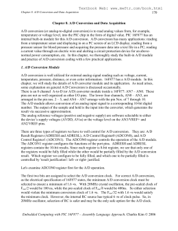
MAPPING AND UNDERSTANDING THE MULTIVARIATE AND MULTI-OBJECTIVE OPTIMIZATION BEHAVIOUR OF A SOI CMOS OTA USING GENETIC ALGORITHMS Thiago Turcato do Rego, Salvador Pinillos Gimenez and Carlos Eduardo Thomaz Centro Universitário da FEI, São Bernardo do Campo, São Paulo, Brazil ABSTRACT Analog integrated circuits design is a complex task due to the large number of optimization parameters involved. In this work, we propose the idea of using Genetic Algorithms (GA) to map and understand the multivariate and multiobjective inherent optimization behavior of the SOI CMOS single-end single-stage OTA. Our work uses GA not only to determine the best parameters for a specific OTA’s design target, but also to track the changes of the W and L dimensions of all the OTA’s transistors and investigate how these changes affect the OTA’s optimization process when operating on distinct specific design targets. Our experimental results have been compared to the literature and SPICE simulations have been carried out to validate our GA approach. 1. INTRODUCTION Analog integrated circuits design is a complex task due to the large number of optimization parameters involved, such as the transistor dimensions, given by the channel width (W) and length (L), the values of transconductance over drain current ratio (gm/IDS) and Early voltage (VEA) of each transistor, as well as different design objectives, such as DC bias conditions, open-loop voltage gain (AV0), unit voltage gain frequency (fT), phase margin and slew rate. There are several possible solutions based, for instance, on transistors’ dimensions combinations and inversion regime conditions that can be proposed to achieve specific design targets (DT). In practice, the solution of a DT depends essentially on the experience of the designer [1,2]. In this work, we propose the idea of using GA [10] to map and understand the multivariate and multi-objective inherent optimization behavior of the SOI CMOS OTA, a well-known analog integrated circuit. We are particularly interested in tracking the changes of the W and L dimensions of all the OTA’s transistors and investigate how these changes affect the OTA’s optimization process when operating on high-gain (HG), high-frequency (HF) and Micropower specific design targets. The following three OTA’s operational values have been evaluated simultaneously in the GA optimization process: AV0, fT and current mirror gain (B). 2. SOI CMOS OTA BASIC EQUATIONS Figure 1 shows the SOI CMOS OTA used in this work. In Figure 1, M1, M2, M7, M8, M9 and M10 are SOI nMOSFETs, M3, M4, M5 and M6 are SOI pMOSFETs, and CL is the capacitive load [9]. More specifically, M1 and M2 transistors are defined as the differential pair, whereas the pairs M3–5, M4–6, M7–8 and M9–10 are defined as the current mirrors. The pair M9–10 is responsible for the current bias of the differential pair. Also, Vdd is the voltage supply, vI+ and vIare the differential inputs, Ipol is the current bias, Io is the current output of the current mirror composed of M9 and M10, and IDS1 and IDS2 are the current drain of the differential pair. V dd M5 M3 M4 M6 ∆V D V D2 V D1 M1 ID S1 I D S2 M2 v I- vO v I+ I O /2 I O /2 I p ol M7 CL M9 I O = I p ol M 10 M8 G nd Figure 1. SOI CMOS OTA schematics. The current mirror gain of M4 and M6 is given by the following equation [6]: W6 B= L6 W4 (1) L4 where L4 and L6 are the channel lengths and W4 and W6 are the channel widths for M4 and M6, respectively. The open-loop voltage gain of the SOI CMOS OTA can be calculated as [6]: g V .V A V 0 = B. m EA 6 EA8 + I V V EA8 DS EA 6 (2) where gm/IDS is the transconductance over drain current ratio of M1 or M2, and VEA6 and VEA8 are the Early voltages for M6 and M8, respectively. The unit voltage gain frequency is then given by : g I . f T = B. m DS (3) I DS 2 πC L Equations (1)–(3) form the basis of our GA approach described in the next section. 3. OUR GA APPROACH GA is a well-known Artificial Intelligence optimization technique based on the principles of natural selection and evolution [10]. There are a number of works that apply GA in analog integrated circuits optimization [2-5,12]. For instance, the work described in [3] applies GA for complex filters designing, such as asymmetric filters, using frequency response analysis to evaluate the circuit. In [4], a similar work to ours is presented where the authors apply GA in an operational transconductance amplifier design, but with different evaluation function and schematic. In [12], the authors have proposed a multi-objective genetic optimization based on Pareto-optimal design points for analog integrated circuits. However, to the best of our knowledge, this is the first study that uses GA not only to determine the best W/L parameters for a specific OTA’s DT, but also to map and understand the multivariate and multi-objective behaviors of such optimization process using these parameters exclusively. Since our GA evaluation process is based on the gm/IDS x IDS/(W/L) methodology of analog integrated circuits design [7], it is necessary to determine firstly the dissipation power (P) and Vdd in order to define the transistors inversion regimes and DC bias conditions. Besides those parameters, the analog integrated circuits designer needs to specify the VEAxL and gm/IDS x IDS/(W/L) curves of the technology to be optimized, as well as the OTA design targets for AV0, fT and B. 3.1. Chromosome Representation Figure 2 shows the chromosome representation of our GA approach. All the W and L alleles are binary numbers composed of 11 bits. Each chromosome (or individual) is evaluated using the AV0, fT and B functions described previously in the basis-equations (1)–(3). Since M1=M2, M3=M4, M5=M6 and M7=M8, it is important to note that the M8 channel width (W8) is not represented in our chromosome because all the basis-equations do not take this parameter into account in their respective formulas. In fact, W8 determines the output node DC bias condition and will be considered during the SPICE simulation only. W2 W4 W6 L2 L4 L6 L8 Figure 2. Chromosome representation. 3.2. Fitness Function To allow a symmetric and monotonically decreasing evaluation of all the individuals, that is, individuals that represent solutions close to the AV0, fT and B specific DTs should have higher values than those far from the aforementioned DTs, we have adopted the Gaussian evaluation functions described in our previous work [11] for the open-loop gain, unit voltage gain frequency and current mirror gain for each GA individual, considering the respective targets specified by the designer before the optimization. The fitness function of our GA optimization process is very simple and defined as an arithmetic mean of all these evaluations. Therefore, all the three objectives have the same weight on the GA fitness function and the individuals that fit better all the three objectives simultaneously will receive higher evaluations in the optimization process. 3.3. GA Optimization Process Firstly, the algorithm generates an initial population with random values for W and L. Once an initial population has been created, each individual is evaluated taking into account the design targets specified. The best evaluated individual is saved in memory to be used further, in the elitism process. Next, the selection process is carried out. This process selects pairs of individuals used in the reproduction process. Individuals have been selected using the wellknown roulette method [?,10]. In the roulette method, solutions with better evaluations have more chance to be selected for reproduction than the others. In this step of the algorithm, the W and L alleles of the selected individuals are swapped using the one-point crossover [10]. The rate of this reproduction process (crossover rate) is an input parameter of the algorithm and has to be set by the designer. Then, the mutation of some individuals occurs. In our binary chromosome representation, this mutation step essentially flips some bits that compose the W and L alleles. Analogously to the crossover rate, the mutation rate is an input parameter and has to be set by the designer as well. After selection, reproduction, mutation and elitism, a new generation is created [11]. GA keeps processing the new generations until reaching the total number of individuals defined by the designer. The total number of individuals is an input parameter and represents the total of individuals that has to be generated by the algorithm, considering that each generation creates new individuals. A new run means starting the GA process of evolution again with a new randomly generated population. The designer has to choose the number of runs and, as larger is this number of runs, more possible solutions are presented at the end of GA optimization process. 4. GA EXPERIMENTS AND RESULTS The GA process was applied for three different OTA operational modes or design targets, that is, HG, HF and Micropower applications, following the reference [6], as indicated in Table I. Table I: OTAs specific design targets. OTA Design Target VDD (V) Ptot (W) -6 AV0 (dB) fT (MHz) Micropower 1.2 5.10 44 0.35 High Gain (HG) 2 100.10-6 65 1.8 High Frequency (HF) 4 30.10-3 35 93 The CL parameter was considered equal to 10pF. The range values of W and L were 1 to 1000µm and 1 to 20µm, respectively, in order to limit the GA searching space of solutions and avoid unpractical solutions (i.e., dimensions smaller than minimal dimensions of the rather than to the differential pair in order to attain the desired AV0 and fT values [6]. In addition, for Micropower OTA, the differential pair must be biased in moderate inversion regime in contrast to pMOSFETs current mirrors, which must be biased in weak inversion regime, according to the reference [6]. Therefore, when we have to design an HF OTA, the pMOSFETs current mirrors must be biased more in the strong inversion regime than in the differential pair, in contrast to HG and Micropower OTAs, regarding the desired AV0 and fT values considered. Since B=1, to achieve the desired AV0 and fT values of the studied OTAs, the behaviors of pMOSFET current mirrors have been optimized generating approximately the same relative values (Figures 3.e and 3.f). Channel Length (L) (µm) 16 14 M ic ro p o w e r O T A L2 L4 L6 L8 12 10 8 6 4 2 0 1x10 4 4 2x10 3x10 4 4x10 4 N u m b e r o f in d iv id u a ls (a) Channel Width (W) (µm) 900 800 700 600 500 HF 400 HG W2 W4 W6 300 200 0 1x10 4 2x10 4 3x10 4 4x10 4 Num ber of individuals (b) Channel Width (W) (µm) 800 700 M ic ro p o w e r O T A W2 W4 W6 600 500 400 300 200 0 1x10 4 2x10 4 3x10 4 4 x1 0 4 4x10 4 N u m b e r o f in d iv id u a ls (c) 700 600 500 W/L technology investigated or too much large). The GA mutation and crossover rates were defined as 9% and 65%, respectively. Moreover, the GA optimization process was set to perform 20 runs with a maximum of 100,000 total individuals. The B value was defined equal to 1 for all design targets in our GA optimization process. To map and understand the GA convergence behavior, Figure 3 presents the tracking of the changes on the OTA’s parameters L (Figure 3.a and 3.b), W (Figure 3.c and 3.d), W/L (Figure 3.e and 3.f), and IDS/(W/L) (Figure 3.g) during optimization, for all the operational modes considered, as a function of the number of individuals. Analyzing these results in details, the following observations can be made. Since AV0 depends on the product over sum ratio of M6 and M8 Early voltages, the GA optimization process in the HG OTA has defined its channel lengths (approximately 20µm for both transistors) with the largest values, in comparison to HF and Micropower, maximizing the M6 and M8 Early voltages. It is important to note that the M8 L of HF is larger than M8 L in the Micropower, because the HF differential pair (M1 and M2) is in the strong inversion regime (Figure 3.h) and, consequently, it presents a lower gm/IDS than the M1 and M2 of the Micropower OTA, which are in the weak inversion regime (large gm/IDS values in relation to HG OTA). For OTAs with high voltage gain approach (HG and Micropower), the pMOSFETs current mirrors (M3/M5 and M4/M6) must present larger W/L values than the differential pair, in contrast to HF OTAs, as indicated in Figures 3.e and 3.f. We believe that this is important design information, but not reported in the literature yet. The W and L values are found by GA optimization process considering the design target that B=1. The W range values are approximately from 250 to 800µm, according to [6]. It is important to emphasize that the W values obtained with our GA optimization process cannot be compared with the W values of reference [6], because our GA approach has not implemented the source by transistors dimensions regarding smallest OTA die area. Analyzing Figure 3.g, and given the AV0 and fT conditions shown in Table I, the differential pair of HF OTA must be biased in the end of moderate inversion regime, near to strong inversion regime, in contrast to pMOSFETs current mirrors (M3-M6). In fact, the pMOSFETs current mirrors must be biased in the strong inversion, in order to reach high frequency response [6]. On the other hand, for HG OTA, the differential pair of the pMOSFETs current mirrors must be biased in the moderate inversion regime, but pMOSFETs current mirrors must be biased nearest to the strong inversion regime HF M ic r o p o w e r W 2 /L 2 400 W 4 /L 4 W 6 /L 6 300 200 100 0 0 1x10 4 2 x10 4 N u m b e r o f in d iv id u a ls (d) 3 x10 4 to be used to predict all transistor dimensions at once and performing a few others iterations with SPICE simulator, we believe that it is possible to generate automatically better solutions, reducing significantly the design time and cost of analog integrated circuits. 40 36 HG W 2 /L 2 W/L 32 W 4 /L 4 28 W 2 /L 2 24 20 Table II: SPICE simulations regarding AV0 and fT targets. 16 0 1 x1 0 4 2x10 4 3 x1 0 4 4x10 4 N u m b e r o f in d iv id u a ls OTA Specific Designs fT target (MHz) fT SPICE (MHz) AV0 target (dB) AV0 SPICE (dB) Micropower High Gain (HG) High Frequency (HF) 0.35 1.8 93 0.3 1.1 180 44 65 35 64 82 53 (e) 10 D iffe re n tia l p a ir (M 1 ,M 2 ) -4 -5 10 -6 C u rre n t M irro rs T ra n s is to rs M 5 ,M 6 S tro n g In v e rs io n HF HG 10 -7 10 -8 10 -9 M ic ro p o w e r Inversion 10 Moderate IDS / (W / L) (A) C u rre n t M irro rs T ra n s is to rs M 3 ,M 4 W eak In ve rsio n 0 .0 2 .0 x1 0 4 4 .0 x1 0 4 6 .0 x1 0 4 8 .0 x1 0 4 1 .0 x 1 0 5 N u m b e r o f in d iv id u a ls (f) Figure 3. HF, HG and Micropower GA optimization changes. 5. SPICE Simulations In order to validate the transistors dimensions obtained by the GA optimization, SPICE simulations were performed. Figure 4 illustrates the Bode plot of the W and L parameters optimized by our GA approach. Voltage Gain (AV0) (dB) 90 O TA HG HF M icroPw 80 70 60 50 40 30 20 10 0 1 10 100 1k 10k 100k 1M 10M 100 M 1G Frequency (H z) Figure 4. Bode plotter of HF, HG and Micropower OTAs. Table II presents the simulated AV0 and fT results of HG, HF and Micropower OTAs, which all transistors are biased in the saturation region and OTA Vout is biased around of Vdd/2. As can be seen, despite the fact that the GA evaluation function has been defined with equals weights for AV0 and fT, the SPICE simulation results indicate that GA optimization process was able to reach satisfactory fT values regarding logarithmic scale, but overestimated the desired OTA AV0. The large differences between desired and simulation OTA AV0 can be explained by the fact that we have used AV0 and fT first order equations to perform the optimization. Besides that, it is important to note that HF OTA presents AV0 and fT values larger than those of reference [6], resulting in a differential pair W obtained by the GA optimization around 2 times larger than that of reference [6]. Thus, we can degrade AV0 and fT by reducing differential pair W dimensions in order to reach the dimensions described in reference [6]. Additionally, thinking in an automatic tool of analog integrated circuits design 6. CONCLUSION This paper proposed the use of Genetic Algorithms to automate the analog integrated circuits design, a complex optimization task dependent mostly on the expertise of the analog designer. More importantly, this work focused on mapping and understanding the transistors dimensions and inversion regimes conditions for different OTA design targets, highlighting important design information. We believe that this proposed tool can reduce significantly the time and cost of analog integrated circuits design, providing relevant information about the inherent multivariate and multi-objective OTA behavior. 7. REFERENCES [1] R.S. Zebulum et. al. Evolutionary Electronics: Automatic Design of Electronic Circuits and Systems by Genetic Algorithms, USA: CRC, 2002. [2] C. Santini, “Desenvolvimento de uma plataforma reconfigurável analógica para a evolução intrínseca de circuitos”. 118 f. Masters Thesis, Electrical Engineering Department, PUC-Rio, 2001 [3] S. Ando, H. Iba . Analog Circuit Design with a Variable Length Cromossome. IEEE Proceeding of the 2000 Congress on Evolutionary Computation”, USA, p 994-1001, 2000. [4] M. Wójcikowski et. al. System for Optimization of Electronic Circuit Using Genetic Algorithm. ICECS'96, Rodos, Greece, pp. 247-250, October 13-16, 1996. [5] M. Barros et. al, An Evolutionary Optimization Kernel with adaptative Parameters Applied to Analog Circuit Design, ISSCS 2005, pp. 545-548 v.2 July 14-15, 2005. [6] J. P. Eggermont et al., Design of SOI CMOS Operational Amplifiers for Applications up to 300°C. IEEE Journal of Solid-State Circuits, Vol. 31, NO. 2, February 1996. [7] F. Silveira et al., A gm/ID Based Methodology for the Design of CMOS Analog Circuits and Its Application to the Synthesis of a Silicon-on-Insulator Micropower OTA, IEEE Journal of Solid-State Circuits, Vol. 31, No. 9, 1996. [8] Pin su et al., BSIMSOI3.1 MOSFET MODEL, University of California, Bekley, 2003. [9] S. P. Gimenez et al., Gain Improvement in Operational Transcond nce Amplifiers Using Graded-Channel SOI nMOSFETs, Microelectronics Journal, Oxford, United Kingdom, 37 (1), p. 31-37, 2006. [10] D. Goldberg, Genetic Algorithms in Search, Optimization and Machine Learning, Addison-Wesley, 1989. [11] T. T. do Rego et al., Analog Integrated Circuits Design by means of Genetic Algorithms. SForum'08, Brazil, 2008. [12] B. D. Smedt and G. G. E. Gielen, WATSON: Design Space Boundary Exploration and Model Generation for Analog and RF IC Design. IEEE Trans. on Computer-Aided Design of Integrated Circuits and Systems, vol. 22, no. 2, p. 213-224, February 2003.
Download