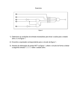
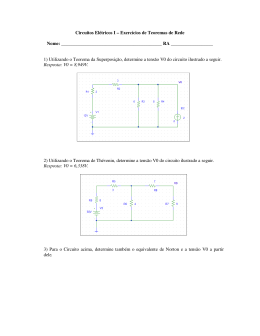
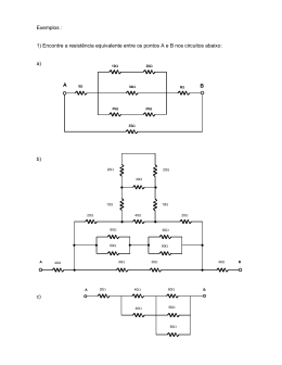
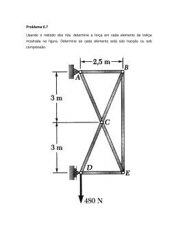
Electrónica II
Exame Normal
18 de Novembro de 2009
9:30-12:30
(Duração: 3 horas)
•
•
•
•
•
•
Universidade do Algarve
MIEET 3º ano
Escreva o seu nome, nº de aluno e curso em todas as folhas que entregar.
Não é permitido falar com os colegas durante o exame. Se o fizer, terá a prova
anulada. Desligue o telemóvel.
Caso opte por desistir, escreva “Desisto”, assine e entregue a prova ao docente.
O exame tem 5 perguntas e a cotação de cada aparece entre parêntesis.
Faça letra legível.
Boa sorte!
Pergunta 1 (5 valores)
O amplificador diferencial (par diferencial) baseado em transístores bipolares
mostrado na figura abaixo tem uma fonte de corrente com resistência de saída igual a
RS = 100 kΩ. Os transístores usados tem parâmetros β = 199 e VA = 100 V,
respectivamente o ganho em corrente base-colector e a tensão Early.
a) Determine a polarização do circuito.
b) Determine o (double-ended) ganho em modo comum e modo diferencial e o
common-mode rejection ratio (CMRR).
Pergunta 2 (2 valores)
O espelho de corrente da figura acima é composto por dois transístores bipolares npn
iguais com parâmetros β = 150 e VA = 100 V.
Calcule o valor exacto da corrente IC e da tensão VC. Assume uma tensão VBE = 0.7 V.
Pergunta 3 (5 valores)
Um amplificador comercial tem os seguintes parâmetros
• Ganho em tensão: A = −100 V/V.
• Resistência de entrada: rin = 5 kΩ.
• Resistência de saída: rout = 1 kΩ.
• Capacidade entre a entrada e a saída: Cf = 10 pF.
• Capacidade entre a entrada e a caixa (terra) e a saída e a caixa (terra): Ci = Co
= 10 pF.
Em base deste amplificador foi desenhado o circuito abaixo
RS = 1 kΩ, RL = 3 kΩ, CS = CL = 10 μF.
a) Determine o ganho em médias frequências do circuito total.
b) Desenhe esquematicamente gráficos Bode do comportamento do circuito em
frequência.
c) Determine a largura de banda do circuito.
Pergunta 4 (5 valores)
Um amplificador operacional (amp-op) é usado num circuito de realimentação
negativa. O factor de realimentação, β, não é constante, mas sim depende da
frequência; β é 100% em baixas frequências e tem pólos em 10 Hz e 1 kHz. O amp-op
é ideal, embora de ter um ganho em malha aberta limitada a 106, independente da
frequência.
a) Derive a expressão do ganho do circuito com realimentação negativa, Af ≡ Vo/Vi.
b) Faça gráficos de Bode e Nyquist para determinar a estabilidade do circuito.
b2) Indique no gráfico de Nyquist o critério de Barkhausen (BC), a zona de
oscilações (OSC), e a zona de perigo de oscilações, com uma margem de fase
igual a 45o, (MF).
b3) Em base dos gráficos, determine se o circuito é estável (não corre o risco de
oscilar). Assume uma margem de fase igual a 45o.
c) Caso não, dê a gama de frequências de (perigo de) oscilação e dê uma maneira de
estabilizar o circuito para evitar possíveis oscilações. Caso sim, dê valores dos
parâmetros que tornam o circuito instável.
Pergunta 5 (3 valores)
O andar de saída da figura ao lado é composto
por um simples transístor junção bipolar npn (β
= 99) e resistências.
a) Qual é a classe do andar?
b) O que será uma boa escolha para o valor da
resistência RB?
c) Calcule a eficiência máxima da potência (η)
deste andar.
d) Com transístores do tipo da tabela abaixa,
será que o transístor sobreaquece com sinal
máximo à saída?
Temperatura máxima da junção
Tj,max
150oC
Temperatura da ambiente
Tamb
40oC
Resistência térmica do pacote
θp
40oC/W
------------------- fim -----------------------
Electronics II
Normal Exam
18 / XII / 2009, 9:30-12:30
(Duration: 3 hours)
•
•
•
•
•
•
Universidade do Algarve
MIEET 3º ano
Write your name, student number and course on all sheet you hand in.
Talking is not allowed. If you do it, your exam will be canceled. Switch off your
cellular telephone.
If you give up, write “I Desist” on the exam sheet and hand it in.
The exam has 5 questions and the maximum score for each is written in brackets.
Write legible.
Good luck!
Question 1 (5)
The figure below shows a differential amplifier (differential pair) based on bipolar
transistors and has a current source with an output resistance equal to RS = 100 kΩ.
The parameters of the transistors are β = 199 e VA = 100 V, respectively the (basecollector) current gain and the Early voltage.
a) Determine the bias point of the circuit.
b) Determine the (double-ended) voltage gain in common mode and differential mode
and the common-mode rejection ratio (CMRR).
Question 2 (2)
The current souce above is composed of two equal bipolar npn transistors with β =
150 e VA = 100 V.
Calculate the exact value of the current IC and the voltage VC. Assume a voltage drop
VBE = 0.7 V.
Question 3 (5)
A certain commercial amplifier has the following parameters
• Voltage gain: A = −100 V/V.
• Input resistance: rin = 5 kΩ.
• Output resistance: rout = 1 kΩ.
• Capacitance between the input and output: Cf = 10 pF.
• Capacitance between the input and the box (ground) and the output and the
box (ground): Ci = Co = 10 pF.
Based on this amplifier the following circuit was designed
RS = 1 kΩ, RL = 3 kΩ, CS = CL = 10 μF.
a) Determine the mid-frequency gain of the complete circuit.
b) Schematically draw Bode plots of the behavior of the circuit in terms of frequency.
c) Determine the band-width of the circuit.
Question 4 (5)
An operational amplifier (op-amp) is used in a circuit with negative feedback. The
feedback factor, β, is not constant, but depends on the frequency; β is 100% at low
frequencies and has two poles, one at 10 Hz and one at 1 kHz. The op-amp is ideal,
apart from the fact that it has an open-loop gain limited to 106, independent of the
frequency.
a) Derive a general expression of the gain of a circuit with negative feedback, Af ≡
Vo/Vi.
b) Draw Bode and Nyquist plots to determine the stability of the circuit.
b2) Indicate in the Nyquist plot the Barkhausen criterion (BC), the zone where
oscillations will occur (OSC), and the zone where oscillations might occur with
a phase margin equal to 45o (PM).
b3) Based on those plots, determine if the circuit is stable (doesn't run the risk of
oscillations). Assume a phase margin equal to 45o.
c) If answer at question b3) is 'not', then give the range of frequencies where
oscillations might occur and a way how to stabilize the circuit to avoid possible
oscillations. If 'yes', give values of the parameters that make the circuit marginally
stable.
Question 5 (3)
The output stage of the figure is made of simple
type npn bipolar junction transistors (β = 99)
and resistances.
a) What is the class of the stage?
b) What would be a good choice for the value
of the resistance RB?
c) Calculate the maximum power efficiency (η)
of this stage.
d) If transistors with thermal parameters as
given in the table below were used, would they
overheat when a maximum output signal
occurs?
Maximum junction temperature
Tj,max
150oC
Ambient temperature
Tamb
40oC
Thermal resistance of the package θp
40oC/W
------------------- end -----------------------
Baixar